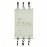
TLP719(TP,F) Toshiba, TLP719(TP,F) Datasheet - Page 2
TLP719(TP,F)
Manufacturer Part Number
TLP719(TP,F)
Description
IC PHOTOCOUPLER IRED 6SMD
Manufacturer
Toshiba
Specifications of TLP719(TP,F)
Number Of Channels
1
Input Type
DC
Voltage - Isolation
5000Vrms
Current Transfer Ratio (min)
20% @ 16mA
Voltage - Output
20V
Current - Output / Channel
8mA
Current - Dc Forward (if)
25mA
Output Type
Transistor with Vcc
Mounting Type
Surface Mount
Package / Case
6-SMD
Lead Free Status / RoHS Status
Lead free / RoHS Compliant
Vce Saturation (max)
-
Current Transfer Ratio (max)
-
Other names
TLP719(TPF)TR
TLP719FTR
TLP719FTR
TLP719FTR
TLP719FTR


Absolute Maximum Ratings
Operating temperature range
Storage temperature range
Lead soldering temperature (10 s)
Isolation voltage (AC, 1 minute, R.H.≤ 60 %)
Note: Using continuously under heavy loads (e.g. the application of high temperature/current/voltage and the
Note 1: Derate 0.45 mA / °C above 70 °C.
Note 2: 50% duty cycle, 1 ms pulse width.
Note 3: Pulse width ≤ 1 μs, 300 pps.
Note 4: Derate 0.8 mW / °C above 70 °C.
Note 5: Derate 1.8 mW / °C above 70 °C.
Note 6: Device considered a two-terminal device: pins 1, 2 and 3 paired with pins 4, 5 and 6 respectively.
Note 7: A ceramic capacitor (0.1 μF) should be connected from pin 6 to pin 4 to stabilize the operation of the
Forward current
Pulse forward current
Peak transient forward current
Reverse voltage
Diode power dissipation
Junction temperature
Output current
Peak output current
Output voltage
Supply voltage
Output power dissipation
Junction Temperature
significant change in temperature, etc.) may cause this product to decrease in the reliability significantly even
if the operating conditions (i.e. operating temperature/current/voltage, etc.) are within the absolute maximum
ratings.
Please design the appropriate reliability upon reviewing the Toshiba Semiconductor Reliability Handbook
(“Handling Precautions”/“Derating Concept and Methods”) and individual reliability data (i.e. reliability test
report and estimated failure rate, etc).
Derate 0.9 mA / °C above 70 °C.
high-gain linear amplifier. Failure to provide the bypassing may impair the switching property.
The total lead length between capacitor and coupler should not exceed 1 cm.
Characteristic
(Ta = 25 °C)
2
(Note 4)
(Note 5)
(Note 1)
(Note 2)
(Note 3)
(Note 6)
Symbol
T opr
I
V
T stg
T sol
BV
I
I
FPT
V
P
V
P
OP
FP
T j
I
T j
I
CC
O
F
O
O
R
D
S
−55~100
−55~125
−0.5~20
−0.5~30
Rating
5000
125
100
125
260
25
50
45
16
1
5
8
Vrms
Unit
mW
mW
mA
mA
mA
mA
°C
°C
°C
°C
°C
A
V
V
V
2007-10-01
TLP719
Related parts for TLP719(TP,F)
Image
Part Number
Description
Manufacturer
Datasheet
Request
R

Part Number:
Description:
PHOTOCOUPLER HS AUTOMATION 6SDIP
Manufacturer:
Toshiba
Datasheet:
Part Number:
Description:
PHOTOCOUPLER HS TRANS-OUT 6SMD
Manufacturer:
Toshiba
Datasheet:

Part Number:
Description:
Microprocessor System Interfaces
Manufacturer:
Toshiba America Electronic Components, Inc.
Datasheet:

Part Number:
Description:
Toshiba Semiconductor [TOSHIBA IGBT Module Silicon N Channel IGBT]
Manufacturer:
TOSHIBA Semiconductor CORPORATION
Datasheet:
Part Number:
Description:
TOSHIBA GTR MODULE SILICON NPN TRIPLE DIFFUSED TYPE
Manufacturer:
TOSHIBA Semiconductor CORPORATION
Datasheet:
Part Number:
Description:
TOSHIBA GTR Module Silicon N Channel IGBT
Manufacturer:
TOSHIBA Semiconductor CORPORATION
Datasheet:
Part Number:
Description:
TOSHIBA Intelligent Power Module Silicon N Channel IGBT
Manufacturer:
TOSHIBA Semiconductor CORPORATION
Datasheet:
Part Number:
Description:
TOSHIBA INTELLIGENT POWER MODULE SILICON N CHANNEL LGBT
Manufacturer:
TOSHIBA Semiconductor CORPORATION
Datasheet:
Part Number:
Description:
TOSHIBA IGBT Module Silicon N Channel IGBT
Manufacturer:
TOSHIBA Semiconductor CORPORATION
Datasheet:
Part Number:
Description:
TOSHIBA GTR MODULE SILICON N−CHANNEL IGBT
Manufacturer:
TOSHIBA Semiconductor CORPORATION
Datasheet:
Part Number:
Description:
TOSHIBA Intelligent Power Module Silicon N Channel IGBT
Manufacturer:
TOSHIBA Semiconductor CORPORATION
Datasheet:
Part Number:
Description:
TOSHIBA GTR Module Silicon N Channel IGBT
Manufacturer:
TOSHIBA Semiconductor CORPORATION
Datasheet:
Part Number:
Description:
TOSHIBA INTELLIGENT POWER MODULE
Manufacturer:
TOSHIBA Semiconductor CORPORATION
Datasheet:
Part Number:
Description:
TOSHIBA Intelligent Power Module Silicon N Channel IGBT
Manufacturer:
TOSHIBA Semiconductor CORPORATION
Datasheet:
Part Number:
Description:
TOSHIBA Intelligent Power Module Silicon N Channel IGBT
Manufacturer:
TOSHIBA Semiconductor CORPORATION
Datasheet: