TCET1100 Vishay, TCET1100 Datasheet - Page 2
TCET1100
Manufacturer Part Number
TCET1100
Description
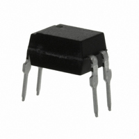
OPTOCOUPLER PHOTOTRANS 600% 4DIP
Manufacturer
Vishay
Specifications of TCET1100
Mounting Type
Through Hole
Isolation Voltage
5000 Vrms
Number Of Channels
1
Input Type
DC
Voltage - Isolation
5000Vrms
Current Transfer Ratio (min)
50% @ 5mA
Current Transfer Ratio (max)
600% @ 5mA
Voltage - Output
70V
Current - Output / Channel
50mA
Current - Dc Forward (if)
60mA
Vce Saturation (max)
300mV
Output Type
Transistor
Package / Case
4-DIP (0.300", 7.62mm)
Maximum Input Diode Current
60 mA
Maximum Reverse Diode Voltage
6 V
Output Device
Transistor
Configuration
1
Maximum Collector Emitter Voltage
70 V
Maximum Collector Emitter Saturation Voltage
300 mV
Current Transfer Ratio
600 %
Maximum Forward Diode Voltage
1.6 V
Maximum Collector Current
50 mA
Maximum Power Dissipation
265 mW
Maximum Operating Temperature
+ 100 C
Minimum Operating Temperature
- 40 C
No. Of Channels
1
Optocoupler Output Type
Phototransistor
Input Current
50mA
Output Voltage
70V
Opto Case Style
DIP
No. Of Pins
4
Approval Bodies
VDE, CSA, BSI EN
Rohs Compliant
Yes
Lead Free Status / RoHS Status
Lead free / RoHS Compliant
Lead Free Status / RoHS Status
Lead free / RoHS Compliant, Lead free / RoHS Compliant
Available stocks
Company
Part Number
Manufacturer
Quantity
Price

Part Number:
TCET1100G
Manufacturer:
VISHAY/威世
Quantity:
20 000


Note
G = lead form 10.16 mm; G is not marked on the body
Notes
(1)
(2)
Document Number: 83503
Rev. 2.3, 14-Oct-09
ORDER INFORMATION
PART
TCET1100
TCET1101
TCET1102
TCET1103
TCET1104
TCET1105
TCET1106
TCET1107
TCET1108
TCET1109
TCET1100G
TCET1101G
TCET1102G
TCET1103G
TCET1104G
TCET1105G
TCET1106G
TCET1107G
TCET1108G
TCET1109G
ABSOLUTE MAXIMUM RATINGS
PARAMETER
INPUT
Reverse voltage
Forward current
Forward surge current
OUTPUT
Collector emitter voltage
Emitter collector voltage
Collector current
Collector peak current
COUPLER
Isolation test voltage (RMS)
Operating ambient temperature range
Storage temperature range
Soldering temperature
T
Stresses in excess of the absolute maximum ratings can cause permanent damage to the device. Functional operation of the device is not
implied at these or any other conditions in excess of those given in the operational sections of this document. Exposure to absolute maximum
ratings for extended periods of the time can adversely affect reliability.
Refer to wave profile for soldering conditions for through hole devices (DIP).
amb
= 25 °C, unless otherwise specified.
(2)
For technical questions, contact:
Optocoupler, Phototransistor Output,
2 mm from case, ≤ 10 s
t
p
TEST CONDITION
/T = 0.5, t
(1)
t
t = 1 min
p
≤ 10 µs
High Temperature
p
≤ 10 ms
optocoupleranswers@vishay.com
SYMBOL
V
V
V
T
I
T
T
I
V
FSM
CEO
ECO
I
CM
amb
I
ISO
stg
sld
F
C
R
CTR 100 % to 200 %, DIP-4, 400 mil
CTR 160 % to 320 %, DIP-4, 400 mil
CTR 100 % to 300 %, DIP-4, 400 mil
CTR 130 % to 260 %, DIP-4, 400 mil
CTR 200 % to 400 %, DIP-4, 400 mil
CTR 50 % to 600 %, DIP-4, 400 mil
CTR 63 % to 125 %, DIP-4, 400 mil
CTR 50 % to 150 %, DIP-4, 400 mil
CTR 80 % to 160 %, DIP-4, 400 mil
CTR 40 % to 80 %, DIP-4, 400 mil
CTR 100 % to 200 %, DIP-4
CTR 160 % to 320 %, DIP-4
CTR 100 % to 300 %, DIP-4
CTR 130 % to 260 %, DIP-4
CTR 200 % to 400 %, DIP-4
TCET1100, TCET1100G
CTR 50 % to 600 %, DIP-4
CTR 63 % to 125 %, DIP-4
CTR 50 % to 150 %, DIP-4
CTR 80 % to 160 %, DIP-4
CTR 40 % to 80 %, DIP-4
Vishay Semiconductors
REMARKS
- 40 to + 100
- 55 to + 125
VALUE
5000
100
260
1.5
60
70
50
6
7
www.vishay.com
UNIT
V
mA
mA
mA
°C
°C
°C
RMS
V
A
V
V
811
Related parts for TCET1100
Image
Part Number
Description
Manufacturer
Datasheet
Request
R

Part Number:
Description:
357-036-542-201 CARDEDGE 36POS DL .156 BLK LOPRO
Manufacturer:
Vishay
Datasheet:
Part Number:
Description:
357-036-542-201 CARDEDGE 36POS DL .156 BLK LOPRO
Manufacturer:
Vishay
Datasheet:
Part Number:
Description:
357-036-542-201 CARDEDGE 36POS DL .156 BLK LOPRO
Manufacturer:
Vishay
Datasheet:
Part Number:
Description:
357-036-542-201 CARDEDGE 36POS DL .156 BLK LOPRO
Manufacturer:
Vishay
Datasheet:
Part Number:
Description:
357-036-542-201 CARDEDGE 36POS DL .156 BLK LOPRO
Manufacturer:
Vishay
Datasheet:
Part Number:
Description:
357-036-542-201 CARDEDGE 36POS DL .156 BLK LOPRO
Manufacturer:
Vishay
Datasheet:
Part Number:
Description:
357-036-542-201 CARDEDGE 36POS DL .156 BLK LOPRO
Manufacturer:
Vishay
Datasheet:
Part Number:
Description:
357-036-542-201 CARDEDGE 36POS DL .156 BLK LOPRO
Manufacturer:
Vishay
Datasheet:
Part Number:
Description:
357-036-542-201 CARDEDGE 36POS DL .156 BLK LOPRO
Manufacturer:
Vishay
Datasheet:
Part Number:
Description:
357-036-542-201 CARDEDGE 36POS DL .156 BLK LOPRO
Manufacturer:
Vishay
Datasheet:
Part Number:
Description:
357-036-542-201 CARDEDGE 36POS DL .156 BLK LOPRO
Manufacturer:
Vishay
Datasheet:
Part Number:
Description:
357-036-542-201 CARDEDGE 36POS DL .156 BLK LOPRO
Manufacturer:
Vishay
Datasheet:
Part Number:
Description:
357-036-542-201 CARDEDGE 36POS DL .156 BLK LOPRO
Manufacturer:
Vishay
Datasheet:
Part Number:
Description:
357-036-542-201 CARDEDGE 36POS DL .156 BLK LOPRO
Manufacturer:
Vishay
Datasheet:
Part Number:
Description:
357-036-542-201 CARDEDGE 36POS DL .156 BLK LOPRO
Manufacturer:
Vishay
Datasheet: