HCPL-4562 Avago Technologies US Inc., HCPL-4562 Datasheet - Page 6
HCPL-4562
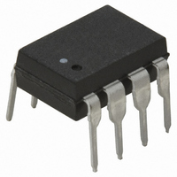
Manufacturer Part Number
HCPL-4562
Description
OPTOCOUPLER HI BAND 17MHZ 8DIP
Manufacturer
Avago Technologies US Inc.
Datasheet
1.HCPL-4562-000E.pdf
(17 pages)
Specifications of HCPL-4562
Input Type
DC
Package / Case
8-DIP (0.300", 7.62mm)
Number Of Channels
1
Voltage - Isolation
3750Vrms
Voltage - Output
20V
Current - Output / Channel
8mA
Current - Dc Forward (if)
12mA
Output Type
Transistor with Vcc
Mounting Type
Through Hole
Isolation Voltage
3750 Vrms
Minimum Forward Diode Voltage
1.1 V
Output Device
Phototransistor
Configuration
1 Channel
Current Transfer Ratio
45 %
Maximum Forward Diode Voltage
1.6 V
Maximum Reverse Diode Voltage
1.8 V
Maximum Input Diode Current
12 mA
Maximum Power Dissipation
100 mW
Maximum Operating Temperature
+ 85 C
Minimum Operating Temperature
- 40 C
Lead Free Status / RoHS Status
Contains lead / RoHS non-compliant
Vce Saturation (max)
-
Current Transfer Ratio (max)
-
Current Transfer Ratio (min)
-
Lead Free Status / RoHS Status
Lead free / RoHS Compliant, Contains lead / RoHS non-compliant
Other names
516-1052-5
Available stocks
Company
Part Number
Manufacturer
Quantity
Price
Company:

Part Number:
HCPL-4562
Manufacturer:
AGILENT
Quantity:
500
Company:
Part Number:
HCPL-4562#500
Manufacturer:
AGILENT
Quantity:
500
Company:
Part Number:
HCPL-4562-000E
Manufacturer:
AVAGO
Quantity:
10 000
Company:
Part Number:
HCPL-4562-020E
Manufacturer:
TI
Quantity:
1 200
Company:
Part Number:
HCPL-4562-020E
Manufacturer:
AVAGO
Quantity:
10 000


IEC/EN/DIN EN 60747-5-2 Insulation Related Characteristics (HCNW4562 ONLY)
*Refer to the front of the optocoupler section of the current catalog, under Product Safety Regulations section IEC/EN/DIN EN
60747-5-2, for a detailed description.
Note: Isolation characteristics are guaranteed only within the safety maximum ratings which must be ensured by protective circuits in
application.
Insulation and Safety Related Specifications
Option 300 - surface mount classification is Class A in accordance with CECC 00802.
6
Parameter
Minimum External
Air Gap (External
Clearance)
Minimum External
Tracking (External
Creepage)
Minimum Internal
Plastic Gap
(Internal Clearance)
Minimum Internal
Tracking (Internal
Creepage)
Tracking Resistance
(Comparative
Tracking Index)
Isolation Group
Description
Installation classification per DIN VDE 0110/1.89, Table 1
Climatic Classification
Pollution Degree (DIN VDE 0110/1.89)
Maximum Working Insulation Voltage
Input to Output Test Voltage, Method b*
Input to Output Test Voltage, Method a*
Highest Allowable Overvoltage*
(Transient Overvoltage, t
Safety Limiting Values
Insulation Resistance at T
V
V
for rated mains voltage ≤ 600 V rms
for rated mains voltage ≤ 1000 V rms
Partial Discharge < 5 pC
t
(Maximum values allowed in the event of a failure,
also see Figure 17, Thermal Derating curve.)
m
IORM
IORM
Case Temperature
Input Current
Output Power
= 60 sec, Partial Discharge < 5 pC
x 1.875 = V
x 1.5 = V
PR
, Type and sample test,
PR
, 100% Production Test with t
ini
S
, V
= 10 sec)
Symbol
L(101)
L(102)
IO
CTI
= 500 V
8-Pin DIP
(300 Mil)
Value
0.08
200
7.1
7.4
NA
IIIa
m
= 1 sec,
Widebody
(400 Mil)
Value
10.0
200
9.6
1.0
4.0
IIIa
Volts
Units
mm
mm
mm
mm
Conditions
Measured from input terminals to
output terminals, shortest distance
through air.
Measured from input terminals to
output terminals, shortest distance
path along body.
Through insulation distance,
conductor to conductor, usually the
direct distance between the photo-
emitter and photodetector inside the
optocoupler cavity.
Measured from input terminals to
output terminals, along internal cavity.
DIN IEC 112/VDE 0303 Part 1
Material Group
(DIN VDE 0110, 1/89, Table 1)
Symbol
P
I
S,OUTPUT
V
V
S,INPUT
V
V
IORM
T
R
IOTM
PR
PR
S
S
Characteristic
55/85/21
1414
2652
2121
8000
≥ 10
150
400
700
I-III
I-IV
2
9
Units
V
V
V
V
mW
mA
°C
Ω
peak
peak
peak
peak
Related parts for HCPL-4562
Image
Part Number
Description
Manufacturer
Datasheet
Request
R

Part Number:
Description:
OPTOCOUPLER PHOTOTRANS 4-SMD
Manufacturer:
Avago Technologies US Inc.
Datasheet:

Part Number:
Description:
OPTOCOUPLER PHOTOTRANS 4-DIP
Manufacturer:
Avago Technologies US Inc.
Datasheet:

Part Number:
Description:
OPTOCOUPLER TRANS-OUT 4-DIP
Manufacturer:
Avago Technologies US Inc.
Datasheet:

Part Number:
Description:
ISOLATOR DGTL 4CH 100MBD 16-SOIC
Manufacturer:
Avago Technologies US Inc.
Datasheet:

Part Number:
Description:
IC,Digital Coupler,CMOS,SOP,16PIN,PLASTIC
Manufacturer:
Avago Technologies US Inc.
Datasheet:
Part Number:
Description:
OPTOCOUPLER HIGH SPEED 16SOIC
Manufacturer:
Avago Technologies US Inc.
Datasheet:

Part Number:
Description:
OPTOCOUPLER AC/DC LOGIC 8DIP
Manufacturer:
Avago Technologies US Inc.
Datasheet:
Part Number:
Description:
OPTOCOUPLER AC/DC LOGIC 8-DIP
Manufacturer:
Avago Technologies US Inc.
Datasheet:
Part Number:
Description:
IC,DIGITAL COUPLER,CMOS,SOP,16PIN,PLASTIC
Manufacturer:
Avago Technologies US Inc.
Datasheet:
Part Number:
Description:
IC,Digital Coupler,CMOS,SOP,16PIN,PLASTIC
Manufacturer:
Avago Technologies US Inc.
Datasheet:

Part Number:
Description:
OPTOCOUPLER PHOTOTRANS 4-SMD GW
Manufacturer:
Avago Technologies US Inc.
Datasheet:

Part Number:
Description:
OPTOCOUPLER PHOTOTRANS 4-MINIPAK
Manufacturer:
Avago Technologies US Inc.
Datasheet:

Part Number:
Description:
OPTOCOUPLER TRANS-OUT 4-DIP
Manufacturer:
Avago Technologies US Inc.
Datasheet:
Part Number:
Description:
OPTOCOUPLER PHOTOTRANS 4-MINIPAK
Manufacturer:
Avago Technologies US Inc.
Datasheet:

Part Number:
Description:
OPTOCOUPLER PHOTOTRANS 4-MINIPAK
Manufacturer:
Avago Technologies US Inc.
Datasheet: