M0220SD-202SDAR1 Newhaven Display, M0220SD-202SDAR1 Datasheet - Page 14
M0220SD-202SDAR1
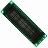
Manufacturer Part Number
M0220SD-202SDAR1
Description
MODULE VF CHAR 2X20 5.34MM
Manufacturer
Newhaven Display
Datasheet
1.M0220SD-202SDAR1.pdf
(22 pages)
Specifications of M0220SD-202SDAR1
Outline L X W X H
116.00mm x 37.00mm x 17.50mm
Viewing Area
70.80mm L x 11.50mm W
Display Format
20 x 2
Display Type
Character
Format
5 x 8 Dots
Voltage - Supply
5V
Character Size
5.34mm H x 2.35mm W
Operating Temperature
-40°C ~ 85°C
Product
Character Display Modules
Character Count X Line
20 x 2
Module Size (w X H X T)
116 mm x 37 mm x 17.5 mm
Voltage Rating
5 V
Operating Temperature Range
- 40 C to + 85 C
Dot Format
5 x 8
Viewing Area (w X H)
70.8 mm x 11.5 mm
Lead Free Status / RoHS Status
Lead free / RoHS Compliant
Interface
-
Number Of Dots
-
Lead Free Status / Rohs Status
Lead free / RoHS Compliant


4-3-1 CHARACTER GENERATOR RAM (CGRAM)
The CGRAM stores the pixel information (1 = pixel on, 0 = pixel off) for the eight user-
definable 5x8 characters. Valid CGRAM addresses are 00H to 3FH. CGRAM not being used to
define characters can be used as general purpose RAM (lower 5 bits only). Character codes 00H
to 07H (or 08H to 0FH) are assigned to the user-definable characters (see section 5.0 Character
Font Tables). The table below shows the relationship between the character codes, CGRAM
addresses, and CGRAM data for each user-definable character.
4-3-2 INSTRUCTIONS
x = don’t care
Clear display
Cursor home
Entry mode set
Display on/off control
Cursor/display shift
Function set
CGRAM address set
DDRAM address set
Address counter read
DDRAM or CGRAM write
DDRAM or CGRAM read
Instruction
x = don't care
D7
0
0
0
D6
0
0
0
Character code
D5
0
0
0
D4
0
0
0
D3
X
X
X
D2
0
0
1
D1
0
0
1
RS
D0
0
1
1
0
0
0
0
0
0
0
0
0
1
1
A5
0
0
1
R/W DB7 DB6 DB5 DB4 DB3 DB2 DB1 DB0
CGRAM address
A4
0
0
0
0
0
0
0
0
1
0
1
0
0
1
A3
0
1
1
BF=0
A2
PAGE: 11/19
0
0
0
0
0
0
0
0
0
0
0
0
1
1
1
1
1
1
1
1
1
1
1
1
0
0
0
0
0
0
0
1
A1
0
0
1
1
0
0
1
1
0
0
1
1
0
0
1
1
0
0
1
1
0
0
1
1
A0
0
0
0
0
0
0
0
0
0
0
0
0
1
1
1
1
1
1
1
1
1
1
1
1
0
0
0
0
0
0
1
D7
X
X
X
D6
X
X
X
0
0
0
0
0
1
D5
X
X
X
CGRAM data
D4
1
1
0
0
1
0
0
0
1
0
1
1
1
1
1
1
1
1
1
1
1
1
0
0
DDRAM address
Write data
D3
DL
Read data
1
0
0
0
1
0
1
0
1
0
0
1
0
0
1
1
0
0
0
0
0
0
1
0
0
0
0
0
1
AC contents
D2
1
0
1
CGRAM address
1
0
0
1
0
0
0
1
0
0
1
0
0
1
0
1
0
0
0
0
0
D1
1
0
1
0
0
0
1
0
1
0
0
1
0
0
1
1
0
0
0
0
0
0
1
0
S/C
N
0
0
0
1
D0
1
0
0
1
0
1
1
0
0
0
0
0
1
0
0
0
0
1
0
0
0
0
1
0
CGRAM
CGRAM
CGRAM
R/L
D
x
0
0
1
(1)
(2)
(8)
M0220SD-202SDAR1
BR1 BR0
I/D
C
0
1
x
B
S
1
x
x
Related parts for M0220SD-202SDAR1
Image
Part Number
Description
Manufacturer
Datasheet
Request
R

Part Number:
Description:
MODULE VF CHAR 2X20 5.34MM
Manufacturer:
Newhaven Display
Datasheet:

Part Number:
Description:
MODULE VF CHAR 2X20 5.34MM
Manufacturer:
Newhaven Display
Datasheet:

Part Number:
Description:
DISPLAY VFD ALPHA 1X20 6.5MM
Manufacturer:
Newhaven Display
Datasheet:

Part Number:
Description:
DISPLAY VFD ALPHA 1X16 5MM
Manufacturer:
Newhaven Display
Datasheet:

Part Number:
Description:
DISPLAY VFD 7-SEG 1X9 9.7MM
Manufacturer:
Newhaven Display
Datasheet:

Part Number:
Description:
DISPLAY VFD 7-SEG 1X6 20MM
Manufacturer:
Newhaven Display
Datasheet:

Part Number:
Description:
DISPLAY VFD 7-SEG 1X19 11MM
Manufacturer:
Newhaven Display
Datasheet:

Part Number:
Description:
DISPLAY VFD 7-SEG 1X3 8MM
Manufacturer:
Newhaven Display
Datasheet:

Part Number:
Description:
DISPLAY VFD CUSTOM DVD
Manufacturer:
Newhaven Display
Datasheet:

Part Number:
Description:
DISPLAY VFD CUST AUDIO
Manufacturer:
Newhaven Display
Datasheet:

Part Number:
Description:
DISPLAY VFD CUST AUDIO
Manufacturer:
Newhaven Display
Datasheet:

Part Number:
Description:
DISPLAY VFD 7-SEG 1X5 7.6MM
Manufacturer:
Newhaven Display
Datasheet:

Part Number:
Description:
DISPLAY VFD CUST APPLIANCE
Manufacturer:
Newhaven Display
Datasheet:

Part Number:
Description:
DISPLAY VFD CUSTOM DVD
Manufacturer:
Newhaven Display
Datasheet:

Part Number:
Description:
DISPLAY VFD 7-SEG 1X4 7.6MM
Manufacturer:
Newhaven Display
Datasheet: