HSC-ADC-EVALB-DCZ Analog Devices Inc, HSC-ADC-EVALB-DCZ Datasheet
HSC-ADC-EVALB-DCZ
Specifications of HSC-ADC-EVALB-DCZ


Related parts for HSC-ADC-EVALB-DCZ


HSC-ADC-EVALB-DCZ Summary of contents
Page 1
... Analog Devices high speed ADC evaluation board, a signal source, and a clock source. Once the kit is connected and powered, the evaluation is enabled instantly on the PC. Two versions of the FIFO are available. The HSC-ADC-EVALB used with multichannel ADCs and converters with demulti- plexed digital outputs. The HSC-ADC-EVALB-SC evaluation board is used with single-channel ADCs ...
Page 2
... FIFO 4.1 Supported ADC Evaluation Boards .......................... 6 Theory of Operation ........................................................................ 9 Clocking Description................................................................... 9 SPI Description............................................................................. 9 REVISION HISTORY 2/06—Revision 0: Initial Version Clocking with Interleaved Data................................................ 10 Connecting to the HSC-ADC-FPGA-4/-8 ............................. 10 Connecting to the DEMUX BRD ............................................ 10 Upgrading FIFO Memory......................................................... 10 Jumpers ............................................................................................ 11 Default Settings........................................................................... 11 Evaluation Board ............................................................................ 13 Power Supplies............................................................................ 13 Connection and Setup ............................................................... 13 FIFO Schematics and PCB Layout ...
Page 3
... Connect the FIFO evaluation board to the ADC evaluation board adapter is required, insert the adapter between the ADC evaluation board and the FIFO board. If using the HSC-ADC-EVALB-SC model, connect the evaluation board to the bottom two rows of the 120-pin connector, closest to the installed IDT FIFO chip. If using an ADC with a SPI interface, remove the two 4-pin corner keys so that the third row can be connected ...
Page 4
... The model supports additional features not found when testing a standard evaluation board. When using the modeling capabilities possible to sweep either the analog amplitude or the analog frequency. For more information consult the www.analog.com/hsc-FIFO. Rev Page button, adjacent to the dialog ADC Analyzer User Manual at ...
Page 5
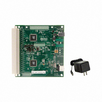
... IDT72V283 32k ⋅ 16-BIT 133MHz FIFO OPEN SOLDER MASK ON ALL DATA AND CLOCK LINES FOR EASY PROBING OPTIONAL SERIAL PORT INTERFACE CONNECTOR HSC-ADC-EVALB-SC/HSC-ADC-EVALB-DC RESET SWITCH µCONTROLLER CRYSTAL WHEN ENCODE RATE IS INTERRUPTED Figure 2. FIFO Components (Top View) Rev Page SWITCHING POWER SUPPLY CONNECTION ON BOARD +3 ...
Page 6
... The evaluation boards in Table 1 can be used with the high speed ADC FIFO evaluation kit. Some evaluation boards require an adapter between the ADC evaluation board connector and the FIFO connector adapter is needed, send an email to highspeed.converters@analog.com with the part number of the adapter and a mailing address. Table 1. HSC-ADC-EVALB-DC- and HSC-ADC-EVALB-SC-Compatible Evaluation Boards Evaluation Board Model Description of ADC ...
Page 7
... DC DC Rev Page Comments Requires HSC-ADC-FPGA-4/-8 Requires AD922xFFA Requires HSC-ADC-FPGA-8 Requires AD922xFFA Requires AD922xFFA Requires HSC-ADC-FPGA-4/-8 Requires HSC-ADC-FPGA-4/-8 Requires AD922xFFA Requires AD922xFFA Requires AD922xFFA Requires HSC-ADC-FPGA-4/-8 Requires AD922xFFA Requires AD922xFFA Requires AD922xFFA Requires AD9283FFA Requires HSC-ADC-FPGA-4/-8 Requires HSC-ADC-FPGA-9289 Requires DEMUX BRD ...
Page 8
... The high speed ADC FIFO evaluation kit can be used to evaluate two channels at a time DEMUX BRD is needed, send an email to highspeed.converters@analog.com. FIFO Board Version Rev Page Comments Requires DEMUX BRD Requires DEMUX BRD Requires GS09066 Requires GS09066 Requires GS09066 Requires GS09066 Requires GS09066 Requires GS09066 Requires GS09066 Requires HSC-ADC-FPGA-4/-8 ...
Page 9
... IDT72V283 FIFO(s), or first pass through the XOR gate timing circuitry described above. SPI DESCRIPTION The Cypress IC (U502) supports the HSC SPI standard to allow programming of ADCs that have SPI-accessible register maps. U102 is a buffer that drives the 4-wire SPI (SCLK, SDI, SDO, ...
Page 10
... This board converts the serial data into parallel CMOS so that the FIFO data capture card can accept the data. For more detailed information on this board, refer to the HSC-ADC-FPGA datasheet at www.analog.com/hsc-FIFO. CONNECTING TO THE DEMUX BRD ADCs that have parallel LVDS outputs require another board that is connected between the ADC evaluation board and the FIFO data capture card ...
Page 11
... Another useful way to configure the jumper settings easily for various configurations is to consult ADC Analyzer under Help > About HSC_ADC_EVALB, and click Set Up Default Jumper Wizard. Then click the configuration setting that applies to the application of interest. A picture of the FIFO board is displayed for that application with a visual of the correct jumper settings already in place. ...
Page 12
... HSC-ADC-EVALB-SC/HSC-ADC-EVALB-DC Single Channel Settings, Default Demultiplexed Jumper # (Bottom) Settings J406 In In J503 In In J504 Out Out J505 In In J506 Out Out J602 Out Out J603 Some jumpers can Ω resistor instead of a physical jumper. This is shown in Table 5 in the jumper description column. ...
Page 13
... ADC evaluation board that supports this feature MAX SWITCHING POWER SUPPLY CHB PARALLEL CMOS OUTPUTS EVALUATION BOARD BAND-PASS XFMR FILTER INPUT CHB PARALLEL CMOS OUTPUTS CLK SPI Rev Page 3.3V – HSC-ADC-EVALB-DC RUNNING FIFO DATA ADC CAPTURE ANALYZER BOARD USB CONNECTION SPI SPI ...
Page 14
... HSC-ADC-EVALB-SC/HSC-ADC-EVALB-DC FIFO SCHEMATICS AND PCB LAYOUT SCHEMATICS E101 VCC WEN1 E102 VCC D1_17 R108 DNP D1_16 WRT_CLK1 R109 D1_15 DNP D1_14 D1_13 D1_12 D1_11 D1_10 D1_9 D1_8 VCC C101 0.1µF PC2 R101 0Ω 1 WEN 2 SEN 3 DNC 4 VCC 5 DNC GND 8 D17 ...
Page 15
... B35 D2_4 D2_3 A36 B36 D2_3 D2_2 A37 B37 D2_2 D2_1 A38 B38 D2_1 D2_0 A39 B39 LSB D2_0 CTRL_D A40 B40 CTRL_D HSC-ADC-EVALB-SC/HSC-ADC-EVALB-DC TEST POINTS PLACEMENT OF HEADER KEY HERE J104 D1_17 C1 D1_17 D1_16 C2 D1_16 C10 C11 C12 C13 C14 C15 ...
Page 16
... HSC-ADC-EVALB-SC/HSC-ADC-EVALB-DC E201 VCC WEN2 1 E202 WEN 2 SEN 3 DNC 4 VCC 5 DNC GND D2_17 8 D17 9 VCC D2_16 10 D16 D2_15 11 D15 D2_14 12 D14 D2_13 13 D13 14 GND D2_12 15 D12 D2_11 16 D11 D2_10 17 D10 D2_9 18 D9 D2_8 VCC U201 VCC R203 DNP WRT_CLK2 R204 DNP VCC ...
Page 17
... HSC-ADC-EVALB-SC/HSC-ADC-EVALB-DC SIDE TOP ON PADS BETWEEN JUMPERS PLACE Figure 8. Schematic (Continued) Rev Page ...
Page 18
... HSC-ADC-EVALB-SC/HSC-ADC-EVALB-DC Figure 9. Schematic (Continued) Rev Page ...
Page 19
... PD4/FD12 Q12 121 PD5/FD13 Q13 122 PD6/FD14 Q14 123 PD7/FD15 Q15 124 RXD1 53 TXD1 52 RXD0 51 TXD0 50 P *WAKEU 101 FF_USB RESET 99 DVCC 2 AVCC 10 Figure 10. Schematic (Continued) Rev Page HSC-ADC-EVALB-SC/HSC-ADC-EVALB- CTL5 98 24.9Ω R515 CTL4 67 24.9Ω R514 CTL3 66 24.9Ω ...
Page 20
... HSC-ADC-EVALB-SC/HSC-ADC-EVALB-DC EXTERNAL MEMORY OVERRIDES ON BOARD MEMORIES WHEN PLUGGED IN. ONLY A SIDE DATA D1_8 DC8 2 15 D1_9 DC9 3 14 D1_10 DC10 4 13 D1_11 DC11 5 12 D1_12 DC12 6 11 D1_13 DC13 7 10 D1_14 DC14 8 9 D1_15 DC15 RZ601 1 16 D1_0 DC0 2 15 D1_1 DC1 ...
Page 21
... PCB LAYOUT HSC-ADC-EVALB-SC/HSC-ADC-EVALB-DC Figure 12. Layer 1—Primary Side Figure 13. Layer 2—Ground Plane Rev Page ...
Page 22
... HSC-ADC-EVALB-SC/HSC-ADC-EVALB-DC Figure 14. Layer 3—Power Plane Figure 15. Layer 4—Secondary Side Rev Page ...
Page 23
... BILL OF MATERIALS Table 6. HSC-ADC-EVALB-SC/HSC-ADC-EVALB-DC Bill of Materials Item Qty Reference Designation 1 42 C101 to C109, C201 to C208, C302, C303, C305, C306, C308, C310, C311, C402 to C405, C503, C506 to C517, C601 2 3 C301, C307, C309 3 2 C312, C313 4 1 C501 5 1 C502 6 2 C504, C505 ...
Page 24
... Y501 49 6 See schematic for placement 50 4 Insert from bottom side of board 51 2 See schematic for placement 1 Only U201 is populated for the single-channel version (HSC-ADC-EVALB-SC). Device Package Description Choke 2020 10 μ 190 Ω @ 100 MHz IC TQFP80 3.3 V, IDT72V283L7-5PF IC SOIC20 74VHC541, ...
Page 25
... Although this product features proprietary ESD protection circuitry, permanent damage may occur on devices subjected to high energy electrostatic discharges. Therefore, proper ESD precautions are recommended to avoid performance degradation or loss of functionality. HSC-ADC-EVALB-SC/HSC-ADC-EVALB-DC Rev Page ...
Page 26
... HSC-ADC-EVALB-SC/HSC-ADC-EVALB-DC NOTES Rev Page ...
Page 27
... NOTES HSC-ADC-EVALB-SC/HSC-ADC-EVALB-DC Rev Page ...
Page 28
... HSC-ADC-EVALB-SC/HSC-ADC-EVALB-DC NOTES ©2006 Analog Devices, Inc. All rights reserved. Trademarks and registered trademarks are the property of their respective owners. EB05870-0-2/06(0) Rev Page ...