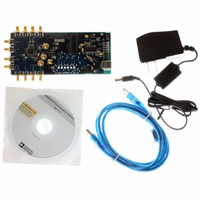
AD9516-4/PCBZ Analog Devices Inc, AD9516-4/PCBZ Datasheet - Page 17

AD9516-4/PCBZ
Manufacturer Part Number
AD9516-4/PCBZ
Description
BOARD EVAL FOR AD9516-4 1.8GHZ
Manufacturer
Analog Devices Inc
Specifications of AD9516-4/PCBZ
Main Purpose
Timing, Clock Generator
Embedded
No
Utilized Ic / Part
AD9516-4
Primary Attributes
2 Inputs, 14 Outputs, 1.6GHz VCO
Secondary Attributes
CMOS, LVDS, LVPECL Output Logic, ADIsimCLK™ Graphical User Interface
Silicon Manufacturer
Analog Devices
Application Sub Type
PLL Clock Synthesizer
Kit Application Type
Clock & Timing
Silicon Core Number
AD9516-0, AD9516-1, AD9516-2
Silicon Family Name
AD9516-X
Rohs Compliant
Yes
Lead Free Status / RoHS Status
Lead free / RoHS Compliant
PIN CONFIGURATION AND FUNCTION DESCRIPTIONS
Table 20. Pin Function Descriptions
Pin No.
1, 11, 12, 30,
31, 32, 38,
49, 50, 51,
57, 60, 61
2
3
4
5
6
7
8
9
10
13
14
Input/
Output
I
I
O
I
O
O
I
I
I
O
I
I
Pin Type
Power
3.3 V CMOS
3.3 V CMOS
Power
3.3 V CMOS
3.3 V CMOS
3.3 V CMOS
3.3 V CMOS
Loop filter
Loop filter
Differential
clock input
Differential
clock input
NC = NO CONNECT
NOTES
1. THE EXTERNAL PADDLE ON THE BOTTOM OF THE PACKAGE MUST BE
2. NC = NO CONNECT. DO NOT CONNECT TO THIS PIN.
REF_SEL
REFMON
BYPASS
STATUS
CONNECTED TO GROUND FOR PROPER OPERATION.
SYNC
SCLK
VCP
CLK
CLK
Mnemonic
VS
REFMON
LD
VCP
CP
STATUS
REF_SEL
SYNC
LF
BYPASS
CLK
CLK
CP
NC
VS
LD
VS
VS
LF
10
11
12
13
14
15
16
1
2
3
4
5
6
7
8
9
PIN 1
INDICATOR
Description
3.3 V Power Pins.
Reference Monitor (Output). This pin has multiple selectable outputs; see Table 54,
Register 0x01B.
Lock Detect (Output). This pin has multiple selectable outputs; see Table 54,
Register 0x1A.
Power Supply for Charge Pump (CP); V
Charge Pump (Output). Connects to external loop filter.
Status (Output). This pin has multiple selectable outputs; see Table 54, Register 0x017.
Reference Select. Selects REF1 (low) or REF2 (high). This pin has an internal 30 kΩ
pull-down resistor.
Manual Synchronizations and Manual Holdover. This pin initiates a manual
synchronization and is also used for manual holdover. Active low. This pin has an
internal 30 kΩ pull-up resistor.
Loop Filter (Input). Connects to VCO control voltage node internally. This pin has
31 pF of internal capacitance to ground, which may influence the loop filter design
for large (>500 kHz) loop bandwidths.
This pin is for bypassing the LDO to ground with a capacitor.
Along with CLK, this is the differential input for the clock distribution section.
Along with CLK, this is the differential input for the clock distribution section.
Figure 6. Pin Configuration
Rev. A | Page 17 of 80
(Not to Scale)
AD9516-4
TOP VIEW
LVPECL LVPECL
LVPECL LVPECL
48
47
46
45
44
43
42
41
40
39
38
37
36
35
34
33
OUT6 (OUT6A)
OUT6 (OUT6B)
OUT7 (OUT7A)
OUT7 (OUT7B)
GND
OUT2
OUT2
VS_LVPECL
OUT3
OUT3
VS
GND
OUT9 (OUT9B)
OUT9 (OUT9A)
OUT8 (OUT8B)
OUT8 (OUT8A)
S
≤ V
CP
≤ 5.0 V.
AD9516-4


