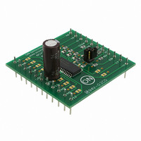
NCV7708AGEVB ON Semiconductor, NCV7708AGEVB Datasheet
NCV7708AGEVB
Specifications of NCV7708AGEVB


Related parts for NCV7708AGEVB

NCV7708AGEVB Summary of contents
Page 1
... Typical Applications • Automotive • Industrial *For additional information on our Pb−Free strategy and soldering details, please download the ON Semiconductor Soldering and Mounting Techniques Reference Manual, SOLDERRM/D. © Semiconductor Components Industries, LLC, 2010 May, 2010 − Rev. 2 http://onsemi.com MARKING DIAGRAM NCV7708A ...
Page 2
EN ENABLE V CC BIAS POR SO SI SPI SCLK CSB VS1 Undervoltage Lockout VS2 VS1 Overvoltage Lockout VS2 VS1 VS CP Charge Pump Control Logic Fault Detect SPI Control Under−load Overcurrent Thermal 16 Bit Warning/Shutdown Logic and Latch VS ...
Page 3
PIN DESCRIPTION Pin No. Symbol 1 OUTL5 Output Low Side 5. Open drain output driver with internal reverse diode. 2 OUTH5 Output High Side 5. Open source output driver with internal reverse diode. Drain connected to VS2. 3 OUTH4 Output ...
Page 4
MAXIMUM RATINGS Power Supply Voltage (VS1, VS2) (DC) (AC), t < 500 ms, Ivsx > −2 A Output Pin OUTHx (DC) (AC – inductive clamping) Output Pin OUTLx (DC) (AC), t < 500 ms, IOUTLx > −2 A (AC Inductive ...
Page 5
ELECTRICAL CHARACTERISTICS (−40°C < T < 150°C, 5.5 V < VSx < < Characteristic GENERAL Supply Current (VS1 + VS2) Sleep Mode (Note 4) Supply Current (VS1) Active Mode Supply Current (V ) − ...
Page 6
ELECTRICAL CHARACTERISTICS (−40°C < T < 150°C, 5.5 V < VSx < < Characteristic OUTPUTS Current Limit (OUTLx) Under Load Detection Threshold (OUTLx) Under Load Detection Threshold (OUTHx) Under Load Detection Delay Time Power ...
Page 7
ELECTRICAL CHARACTERISTICS (−40°C < T < 150°C, 5.5 V < VSx < Characteristic Serial Peripheral Interface ( SCLK Frequency SCLK Clock Period Maximum Input Capacitance (Note 7) SCLK High Time ...
Page 8
CSB 5 SCLK 3 CSB SCLK 10 SO SPI Communication Standard 16−bit communication has been implemented for the communication of this IC to turn drivers on and off, and to report faults. (Reference the SPI Communication Frame ...
Page 9
CSB SI SRR OUTL1 OUTH1 OUTL2 OUTH2 OUTL3 OUTH3 OUTL4 SCLK TW OUTL1 OUTH1 OUTL2 OUTH2 OUTL3 OUTH3 OUTL4 SO The table below defines the programming bits and diagnostic bits. Fault information is sequentially clocked out the SO pin of ...
Page 10
DETAILED OPERATING DESCRIPTION General The NCV7708A Double Hex Driver provides drive capability for 3 independent H−Bridge configurations High Side configurations with 6 Low Side configurations, or any combination of arrangements. Each output drive is characterized for a 500 ...
Page 11
Over Voltage Shutdown Over voltage shutdown circuitry monitors the voltage on the VS1 and VS2 pins. When the Over−voltage Threshold voltage level has been breached on both or either one of the VSx supply inputs, output bit 15 will be ...
Page 12
Applications Drawing The applications drawing below displays the range with which this part can drive a multitude of loads. + OUTHx OUTLx VSx OUTHx OUTLx GND Any combination of motors and high side drivers can be designed in. This allows ...
Page 13
Typical Operating Characteristics −1.2 −1.0 −0.8 −0.6 −0.4 −0 −1.0 −2.0 HIGH SIDE PIN VOLTAGE (V) Figure 6. Typical High−side Negative Clamp Voltage vs. Reverse Current, Room Temperature 110 100 ...
Page 14
0.01 1.0 0.1 2 Cu_Area = 986 0.01 0.000001 0.00001 0.0001 Figure 11. SOIC 28−Lead Thermal Duty Cycle Curves ...
Page 15
The Cauer networks generally have physical significance and may be divided between nodes to separate thermal behavior due to one portion of the network from another. The Foster networks, though when sorted by time constant (as above) bear a rough ...
Page 16
... Opportunity/Affirmative Action Employer. This literature is subject to all applicable copyright laws and is not for resale in any manner. PUBLICATION ORDERING INFORMATION LITERATURE FULFILLMENT: Literature Distribution Center for ON Semiconductor P.O. Box 5163, Denver, Colorado 80217 USA Phone: 303−675−2175 or 800−344−3860 Toll Free USA/Canada Fax: 303− ...