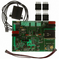
EVAL-ADM1192EBZ Analog Devices Inc, EVAL-ADM1192EBZ Datasheet
EVAL-ADM1192EBZ
Specifications of EVAL-ADM1192EBZ


Related parts for EVAL-ADM1192EBZ


EVAL-ADM1192EBZ Summary of contents
Page 1
FEATURES Powered from 3. Precision current sense amplifier Precision voltage input 12-bit ADC for current and voltage readback ALERT output allows basic P-channel FET hot swap SETV input for setting overcurrent alert ...
Page 2
ADM1192 TABLE OF CONTENTS Features .............................................................................................. 1 Applications....................................................................................... 1 General Description ......................................................................... 1 Functional Block Diagram .............................................................. 1 Revision History ............................................................................... 2 Specifications..................................................................................... 3 Absolute Maximum Ratings............................................................ 5 Thermal Characteristics .............................................................. 5 ESD Caution.................................................................................. 5 Pin Configuration and Function Descriptions............................. ...
Page 3
SPECIFICATIONS −40°C to +85°C, typical values Table 1. Parameter VCC PIN Operating Voltage Range Supply Current Undervoltage Lockout, V UVLO Undervoltage Lockout Hysteresis, ...
Page 4
ADM1192 Parameter SETV PIN Overcurrent Trip Threshold Overcurrent Trip Gain, V /(V − V SETV CC SENSE Input Current, I SETVLEAK Glitch Filter, t SETVGLITCH TIMER PIN Pull-Up Current (Overcurrent Fault), I TIMERUPOC Pull-Down Current, I TIMERDN Pin Threshold High, ...
Page 5
ABSOLUTE MAXIMUM RATINGS Table 2. Parameter VCC Pin SENSE Pin TIMER Pin CLRB Pin SETV Pin ALERT Pin SDA Pin, SCL Pin ADR Pin Storage Temperature Range Operating Temperature Range Lead Temperature (Soldering 10 sec) Junction Temperature Stresses above those ...
Page 6
ADM1192 PIN CONFIGURATION AND FUNCTION DESCRIPTIONS Table 4. Pin Function Descriptions Pin No. Mnemonic Description 1 VCC Positive Supply Input Pin. The operating supply voltage range is 3. undervoltage lockout (UVLO) circuit resets the ADM1192 ...
Page 7
TYPICAL PERFORMANCE CHARACTERISTICS 2.0 1.8 1.6 1.4 1.2 1.0 0.8 0.6 0.4 0 (V) CC Figure 4. Supply Current vs. Supply Voltage 2.0 1.8 1.6 1.4 1.2 1.0 0.8 0.6 0.4 0.2 0 ...
Page 8
ADM1192 –1 –2 –3 –4 0 500 1000 1500 2000 2500 CODE Figure 10. INL for ADC –1 –2 –3 –4 0 500 1000 1500 2000 2500 CODE Figure 11. ...
Page 9
HIGH 1.2 1.0 0.8 0.6 0.4 0 (V) CC Figure 16. Timer Threshold vs. Supply Voltage 2.0 1.8 1.6 1.4 1.2 1.0 0.8 0.6 0.4 ...
Page 10
ADM1192 VOLTAGE AND CURRENT READBACK The ADM1192 contains the components to allow voltage and 2 current readback over bus. The voltage output of the current sense amplifier and the voltage on the VCC pin are fed into ...
Page 11
SCL SDA START BY MASTER FRAME 1 SLAVE ADDRESS 1 SCL (CONTINUED) SDA (CONTINUED) FRAME 3 DATA BYTE 1 SCL SDA START BY MASTER ...
Page 12
ADM1192 WRITE AND READ OPERATIONS 2 The I C specification defines several protocols for different types of read and write operations. The operations used in the ADM1192 are discussed in this section. Table 6 shows the abbreviations used in the ...
Page 13
WRITE EXTENDED COMMAND BYTE In the write extended command byte operation, the master device writes to one of the three extended registers of the slave device, as follows: 1. The master device asserts a start condition on SDA. 2. The ...
Page 14
ADM1192 READ VOLTAGE AND/OR CURRENT DATA BYTES Depending on how the device is configured, ADM1191 can be set up to provide information in three ways after a conversion (or conversions): voltage and current readback, voltage only readback, and current only ...
Page 15
Table 15. Status Byte Operations Bit Name Function 0 ADC_OC An ADC-based overcurrent comparison has been detected on the last three conversions. 1 ADC_ALERT An ADC-based overcurrent trip has occurred, causing the alert. Cleared by writing to Bit 4 of ...
Page 16
ADM1192 APPLICATIONS INFORMATION ALERT OUTPUT The ALERT output is an open-drain pin with 30 V tolerance. There are two uses for this output. Overcurrent Flag The ALERT pin can be connected to the general-purpose logic input of a controller. During ...
Page 17
KELVIN SENSE RESISTOR CONNECTION When using a low value sense resistor for high current measure- ment, the problem of parasitic series resistance can arise. The lead resistance can be a substantial fraction of the rated resistance, making the total resistance ...
Page 18
... ADM1192 OUTLINE DIMENSIONS ORDERING GUIDE Model Temperature Range 1 ADM1192-1ARMZ-R7 −40°C to +85°C EVAL-ADM1192EBZ RoHS Compliant Part. 3.10 3.00 2. 5.15 3.10 4.90 3.00 4.65 2. PIN 1 0.50 BSC 0.95 0.85 1.10 MAX 0.75 0.15 0.33 SEATING 0.23 0.05 PLANE 0.17 0.08 COPLANARITY ...
Page 19
NOTES Rev Page ADM1192 ...
Page 20
ADM1192 NOTES 2 Purchase of licensed I C components of Analog Devices, Inc., or one of its sublicensed Associated Companies conveys a license for the purchaser under the Philips I 2 Patent Rights to use these components ...