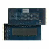
CY8CKIT-029 Cypress Semiconductor Corp, CY8CKIT-029 Datasheet - Page 37

CY8CKIT-029
Manufacturer Part Number
CY8CKIT-029
Description
KIT DEV PSOC3 LCD SEGMENT EXPAN
Manufacturer
Cypress Semiconductor Corp
Series
PSOC™ 3r
Specifications of CY8CKIT-029
Main Purpose
Displays, LCD Display
Embedded
Yes, MCU, 32-Bit
Primary Attributes
128 addressable segments
Secondary Attributes
CD contains sample projects
Description/function
Evaluation Kit
Interface Type
USB
Backlighting
No Backlighting
Data Bus Width
8 bit, 16 bit, 32 bit
Maximum Operating Temperature
+ 50 C
Minimum Operating Temperature
0 C
Number Of Segments
7, 14
Operating Voltage
2.5 V to 5.5 V
Pixel Format
8 x 16
Product
Display Modules
Software
Software Included
Touch Panel
No Touch Panel
For Use With/related Products
PSoC 3
Lead Free Status / RoHS Status
Lead free / RoHS Compliant
Utilized Ic / Part
-
Lead Free Status / Rohs Status
Lead free / RoHS Compliant
Other names
428-2993
Example Projects
Note Pin assignment in both example projects is according to Port A of the DVK. Open the example
project and change the pin assignment in PSoC Creator (in .cydwr file) for Port A' or port B according
to
Table
4-2. The pin assignment for example project 1 is shown in
Figure
5-25.
Figure 5-25. Pin Connection Mapping for Port A'
Note The pins for VR and the SW1 must be reassigned to any other free GPIO when using port A'
and port B. This is because P0_2 pin used in both example projects for VR and SW1, is used for
common lines. In addition, for the StopWatch example project, the port pin used for the switch SW1
has resistive pull up drive mode. This is because the switch SW1 is connected to the switch in the
CY8CKIT-001 DVK. The switch in the DVK is connected to GND when pressed; therefore, the drive
mode must be set to ‘Resistive Pull Up’. Write ‘1’ to the port pin in the firmware to make it work. The
following code indicates the location where you can set this according to the selection of port pin.
/* Write '1' to input switch port pin, P0.2 for enable resistive pull up
*/
CY_SET_REG8 (CYDEV_IO_PRT_PRT0_DR, 0x04);
To use P1_7, modify as shown here:
/* Write '1' to input switch port pin, P1.7 for enable resistive pull up
*/
CY_SET_REG8 (CYDEV_IO_PRT_PRT1_DR, 0x80);
CY8CKIT-029 PSoC LCD Segment Drive Expansion Board Kit Guide, Doc. # 001-55415 Rev. *B
37
[+] Feedback


