MCP3221DM-PCTL Microchip Technology, MCP3221DM-PCTL Datasheet - Page 13
MCP3221DM-PCTL
Manufacturer Part Number
MCP3221DM-PCTL
Description
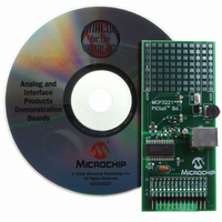
BOARD DEMO FOR PICTAIL MCP3221
Manufacturer
Microchip Technology
Series
PICtail™r
Type
A/Dr
Datasheets
1.MCP3221A5T-IOT.pdf
(28 pages)
2.MCP3221DM-PCTL.pdf
(20 pages)
3.MCP3221DM-PCTL.pdf
(20 pages)
Specifications of MCP3221DM-PCTL
Number Of Adc's
1
Number Of Bits
12
Sampling Rate (per Second)
22.3k
Data Interface
Serial
Inputs Per Adc
1 Single Ended
Voltage Supply Source
Single Supply
Operating Temperature
-40°C ~ 85°C
Utilized Ic / Part
MCP3221
Product
Data Conversion Development Tools
Resolution
12 bit
Interface Type
USB
Silicon Manufacturer
Microchip
Silicon Core Number
MCP3221
Kit Application Type
Data Converter
Application Sub Type
ADC
Silicon Family Name
PICtail
Kit Contents
Board Cables CD Docs
Rohs Compliant
Yes
For Use With/related Products
MCP3221
Lead Free Status / RoHS Status
Contains lead / RoHS non-compliant
Lead Free Status / RoHS Status
Lead free / RoHS Compliant, Contains lead / RoHS non-compliant
Available stocks
Company
Part Number
Manufacturer
Quantity
Price
Company:

Part Number:
MCP3221DM-PCTL
Manufacturer:
MICROCHIP
Quantity:
12 000


4.0
The MCP3221 employs a classic SAR architecture.
This architecture uses an internal sample and hold
capacitor to store the analog input while the conversion
is taking place. At the end of the acquisition time, the
input switch of the converter opens and the device uses
the collected charge on the internal sample-and-hold
capacitor to produce a serial 12-bit digital output code.
The acquisition time and conversion is self-timed using
an internal clock. After each conversion, the results are
stored in a 12-bit register that can be read at any time.
Communication with the device is accomplished with a
2-wire, I
22.3 ksps are possible with the MCP3221 in a continu-
ous-conversion mode and an SCL clock rate of
400 kHz.
4.1
The digital output code produced by the MCP3221 is a
function of the input signal and power supply voltage,
V
reduced accordingly. The theoretical LSB size is shown
below.
EQUATION
The output code of the MCP3221 is transmitted serially
with MSB first. The format of the code is straight binary.
FIGURE 4-1:
© 2006 Microchip Technology Inc.
DD
. As the V
DEVICE OPERATION
Digital Output Code
2
C interface. Maximum sample rates of
DD
V
DD
LSB SIZE
level is reduced, the LSB size is
= Supply voltage
Transfer Function.
0000 0000 0010 (2)
0000 0000 0001 (1)
0000 0000 0000 (0)
0000 0000 0011 (3)
1111 1111 1111
1111 1111 1110
=
V DD
------------
4096
Output Code
.5 LSB
(4095)
(4094)
1.5 LSB
2.5 LSB
4.2
The conversion time is the time required to obtain the
digital result once the analog input is disconnected
from the holding capacitor. With the MCP3221, the
specified conversion time is typically 8.96 µs. This time
is dependent on the internal oscillator and is
independent of SCL.
4.3
The acquisition time is the amount of time the sample
cap array is acquiring charge.
The acquisition time is, typically, 1.12 µs. This time is
dependent on the internal oscillator and independent of
SCL.
4.4
Sample rate is the inverse of the maximum amount of
time that is required from the point of acquisition of the
first conversion to the point of acquisition of the second
conversion.
The sample rate can be measured either by single or
continuous conversions. A single conversion includes
a Start Bit, Address Byte, Two Data Bytes and a Stop
bit. This sample rate is measured from one Start Bit to
the next Start Bit.
For continuous conversions (requested by the Master
by issuing an acknowledge after a conversion), the
maximum sample rate is measured from conversion to
conversion or a total of 18 clocks (two data bytes and
two Acknowledge bits). Refer to Section 5.2 “Device
Addressing”, “Device Addressing”.
V
DD
Conversion Time (t
Acquisition Time (t
Sample Rate
-2.5 LSB
V
DD
-1.5 LSB
AIN
MCP3221
ACQ
CONV
DS21732C-page 13
)
)
Related parts for MCP3221DM-PCTL
Image
Part Number
Description
Manufacturer
Datasheet
Request
R

Part Number:
Description:
Manufacturer:
Microchip Technology Inc.
Datasheet:
Part Number:
Description:
Manufacturer:
Microchip Technology Inc.
Datasheet:
Part Number:
Description:
Manufacturer:
Microchip Technology Inc.
Datasheet:
Part Number:
Description:
Manufacturer:
Microchip Technology Inc.
Datasheet:
Part Number:
Description:
Manufacturer:
Microchip Technology Inc.
Datasheet:
Part Number:
Description:
Manufacturer:
Microchip Technology Inc.
Datasheet:
Part Number:
Description:
Manufacturer:
Microchip Technology Inc.
Datasheet:
Part Number:
Description:
Manufacturer:
Microchip Technology Inc.
Datasheet: