MCP3221DM-PCTL Microchip Technology, MCP3221DM-PCTL Datasheet - Page 2
MCP3221DM-PCTL
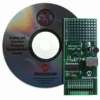
Manufacturer Part Number
MCP3221DM-PCTL
Description
BOARD DEMO FOR PICTAIL MCP3221
Manufacturer
Microchip Technology
Series
PICtail™r
Type
A/Dr
Datasheets
1.MCP3221A5T-IOT.pdf
(28 pages)
2.MCP3221DM-PCTL.pdf
(20 pages)
3.MCP3221DM-PCTL.pdf
(20 pages)
Specifications of MCP3221DM-PCTL
Number Of Adc's
1
Number Of Bits
12
Sampling Rate (per Second)
22.3k
Data Interface
Serial
Inputs Per Adc
1 Single Ended
Voltage Supply Source
Single Supply
Operating Temperature
-40°C ~ 85°C
Utilized Ic / Part
MCP3221
Product
Data Conversion Development Tools
Resolution
12 bit
Interface Type
USB
Silicon Manufacturer
Microchip
Silicon Core Number
MCP3221
Kit Application Type
Data Converter
Application Sub Type
ADC
Silicon Family Name
PICtail
Kit Contents
Board Cables CD Docs
Rohs Compliant
Yes
For Use With/related Products
MCP3221
Lead Free Status / RoHS Status
Contains lead / RoHS non-compliant
Lead Free Status / RoHS Status
Lead free / RoHS Compliant, Contains lead / RoHS non-compliant
Available stocks
Company
Part Number
Manufacturer
Quantity
Price
Company:

Part Number:
MCP3221DM-PCTL
Manufacturer:
MICROCHIP
Quantity:
12 000


MCP3221
1.0
Absolute Maximum Ratings †
V
Analog input pin w.r.t. V
SDA and SCL pins w.r.t. V
Storage temperature .....................................-65°C to +150°C
Ambient temp. with power applied ................-65°C to +125°C
Maximum Junction Temperature .......... .........................150°C
ESD protection on all pins (HBM) .................................≥ 4 kV
DC ELECTRICAL SPECIFICATIONS
DS21732C-page 2
Electrical Characteristics: Unless otherwise noted, all parameters apply at V
T
DC Accuracy
Resolution
Integral Nonlinearity
Differential Nonlinearity
Offset Error
Gain Error
Dynamic Performance
Total Harmonic Distortion
Signal-to-Noise and Distortion
Spurious-Free Dynamic Range
Analog Input
Input Voltage Range
Leakage Current
SDA/SCL (open-drain output):
Data Coding Format
High-level input voltage
Low-level input voltage
Low-level output voltage
Hysteresis of Schmitt trigger inputs
Input leakage current
Output leakage current
Pin capacitance
(all inputs/outputs)
Bus Capacitance
Note 1:
DD
AMB
...................................................................................7.0V
= -40°C to +85°C, I
2:
3:
4:
5:
ELECTRICAL
CHARACTERISTICS
“Sample time” is the time between conversions once the address byte has been sent to the converter.
Refer to Figure 5-6.
This parameter is periodically sampled and not 100% tested.
R
SDA and SCL = V
t
SCL.
Parameters
ACQ
PU
= Pull-up resistor on SDA and SCL.
and t
SS
CONV
.......... ............. -0.6V to V
SS
........... .........-0.6V to V
2
C Fast Mode Timing: f
are dependent on internal oscillator timing. See Figure 5-5 and Figure 5-6 for relation to
SS
to V
DD
SINAD
SFDR
V
C
Sym
THD
DNL
C
V
INL
V
HYST
at 400 kHz.
V
I
C
I
OUT
LO
OL
LI
IN
IH
IL
B
,
DD
DD
V
0.7 V
+0.6V
+1.0V
SCL
SS
Min
—
—
—
—
—
—
—
—
—
—
—
—
-1
-1
-1
-0.3
= 400 kHz (Note 3).
DD
Straight Binary
0.05 V
±0.75
±0.75
±0.5
Typ
-82
72
86
12
—
—
—
—
—
—
—
—
—
-1
† Stresses above those listed under “Maximum ratings” may
cause permanent damage to the device. This is a stress rating
only and functional operation of the device at those or any
other conditions above those indicated in the operational list-
ings of this specification is not implied. Exposure to maximum
rating conditions for extended periods may affect device
reliability.
DD
V
0.3 V
DD
Max
400
0.4
±2
±1
±2
±3
+1
+1
+1
10
—
—
—
—
—
+0.3
DD
DD
Units
LSB
LSB
LSB
LSB
bits
= 5.0V, V
dB
dB
dB
µA
µA
µA
pF
pF
V
V
V
V
V
© 2006 Microchip Technology Inc.
No missing codes
V
V
V
2.7V ≤ V
I
f
V
V
0.9 V
T
(Note 2)
SDA drive low, 0.4V
OL
SCL
AMB
IN
IN
IN
IN
OUT
SS
= 3 mA, R
= 0.1V to 4.9V @ 1 kHz
= 0.1V to 4.9V @ 1 kHz
= 0.1V to 4.9V @ 1 kHz
= 0.1 V
= 400 kHz only
= GND, R
DD
= 25°C, f = 1 MHz;
= 0.1 V
Conditions
DD
DD
≤ 5.5V
SS
PU
and 0.9 V
PU
and
= 1.53 kΩ
= 2 kΩ
DD
Related parts for MCP3221DM-PCTL
Image
Part Number
Description
Manufacturer
Datasheet
Request
R

Part Number:
Description:
Manufacturer:
Microchip Technology Inc.
Datasheet:
Part Number:
Description:
Manufacturer:
Microchip Technology Inc.
Datasheet:
Part Number:
Description:
Manufacturer:
Microchip Technology Inc.
Datasheet:
Part Number:
Description:
Manufacturer:
Microchip Technology Inc.
Datasheet:
Part Number:
Description:
Manufacturer:
Microchip Technology Inc.
Datasheet:
Part Number:
Description:
Manufacturer:
Microchip Technology Inc.
Datasheet:
Part Number:
Description:
Manufacturer:
Microchip Technology Inc.
Datasheet:
Part Number:
Description:
Manufacturer:
Microchip Technology Inc.
Datasheet: