EVAL-AD7731EBZ Analog Devices Inc, EVAL-AD7731EBZ Datasheet - Page 24
EVAL-AD7731EBZ
Manufacturer Part Number
EVAL-AD7731EBZ
Description
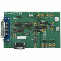
BOARD EVALUATION FOR AD7731
Manufacturer
Analog Devices Inc
Datasheets
1.AD7731BRUZ.pdf
(44 pages)
2.EVAL-AD7731EBZ.pdf
(11 pages)
3.EVAL-AD7731EBZ.pdf
(3 pages)
4.EVAL-AD7731EBZ.pdf
(44 pages)
Specifications of EVAL-AD7731EBZ
Number Of Adc's
1
Number Of Bits
24
Sampling Rate (per Second)
6.4k
Data Interface
Serial
Inputs Per Adc
3 Differential
Input Range
±1.28 V
Power (typ) @ Conditions
67.5mW @ 6.4kSPS
Voltage Supply Source
Analog and Digital
Operating Temperature
-40°C ~ 85°C
Utilized Ic / Part
AD7731
Lead Free Status / RoHS Status
Lead free / RoHS Compliant


AD7731
REFERENCE INPUT
The AD7731’s reference inputs, REF IN(+) and REF IN(–),
provide a differential reference input capability. The common-
mode range for these differential inputs is from AGND to AV
The nominal reference voltage, V
for specified operation is +2.5 V with the HIREF bit at 0 and
+5 V with the HIREF bit at 1. The part is also functional with
V
ing of all input ranges. The resolution in nV will be unaltered,
but will be reduced by 1 bit in terms of peak-to-peak resolution.
Both reference inputs provide a high impedance, dynamic load.
The typical average dc input leakage current is over temperature
is 4.5 A with HIREF = 0 and 8 A with HIREF = 1. Because
the input impedance on each reference input is dynamic, exter-
nal resistance/capacitance combinations may result in gain er-
rors on the part.
The output noise performance outlined in Tables I through IV
is for an analog input of 0 V and is unaffected by noise on the
reference. To obtain the same noise performance as shown in
the noise tables over the full input range requires a low noise
reference source for the AD7731. If the reference noise in the
bandwidth of interest is excessive, it will degrade the perfor-
mance of the AD7731. In applications where the excitation
voltage for the transducer on the analog input also drives the
reference voltage for the part, the effect of the low-frequency
noise in the excitation voltage will be removed as the application
is ratiometric. In this case, the reference voltage for the AD7731
and the excitation voltage for the transducer are the same. The
HIREF bit of the Mode Register should be set to 1.
If the AD7731 is not used in a ratiometric application, a low
noise reference should be used. Recommended reference voltage
sources for the AD7731 include the AD780, REF43 and REF192.
If any of these references are used as the reference source for the
AD7731, the HIREF bit should be set to 0. It is generally rec-
ommended to decouple the output of these references to further
reduce the noise level.
Reference Detect
The AD7731 includes on-chip circuitry to detect if the part has
a valid reference for conversions or calibrations. If the voltage
between the REF IN(+) and REF IN(–) pins goes below 0.3 V
or either the REF IN(+) or REF IN(–) inputs is open circuit,
the AD7731 detects that it no longer has a valid reference. In
this case, the NOREF bit of the Status Register is set to a 1.
If the AD7731 is performing normal conversions and the NOREF
bit becomes active, the part places all 1s in the Data Register.
Therefore, it is not necessary to continuously monitor the status
of the NOREF bit when performing conversions. It is only nec-
essary to verify its status if the conversion result read from the
Data Register is all 1s.
If the AD7731 is performing either an offset or gain calibration
and the NOREF bit becomes active, the updating of the respec-
tive calibration register is inhibited to avoid loading incorrect
coefficients to this register. If the user is concerned about verify-
ing that a valid reference is in place every time a calibration is
performed, then the status of the NOREF bit should be checked
at the end of the calibration cycle.
REF
of +2.5 V with the HIREF bit at 1. This results in a halv-
REF
(REF IN(+) – REF IN(–)),
DD
.
–24–
SIGMA-DELTA MODULATOR
A sigma-delta ADC generally consists of two main blocks, an
analog modulator and a digital filter. In the case of the AD7731,
the analog modulator consists of a difference amplifier, an inte-
grator block, a comparator and a feedback DAC as illustrated in
Figure 7. In operation, the analog signal sample is fed to the
difference amplifier along with the output of the feedback DAC.
The difference between these two signals is integrated and fed to
the comparator. The output of the comparator provides the
input to the feedback DAC so the system functions as a negative
feedback loop that tries to minimize the difference signal. The
digital data that represents the analog input voltage is contained
in the duty cycle of the pulse train appearing at the output of the
comparator. This duty cycle data can be recovered as a data
word using the digital filter. The sampling frequency of the
modulator loop is many times higher than the bandwidth of the
input signal. The integrator in the modulator shapes the quanti-
zation noise (which results from the analog to digital conversion) so
that the noise is pushed towards one half of the modulator fre-
quency. The digital filter then bandlimits the response to a fre-
quency significantly lower than one half of the modulator
frequency. In this manner, the 1-bit output of the comparator
is translated into a bandlimited, low noise output from the
AD7731.
DIGITAL FILTERING
Filter Architecture
The output of the modulator feeds directly into the digital filter.
This digital filter consists of two portions, a first stage filter and
a second stage filter. The cutoff frequency and output rate of
the filter are programmable. The first stage filter is a low-pass,
sinc
quantization noise introduced at the modulator. The second
stage filter has three distinct modes of operation. The first op-
tion is where it is bypassed completely such that the only filter-
ing provided on the AD7731 is performed by the first stage sinc
filter. The second is where it provides a low-pass 22-tap FIR
filter which processes the output of the first stage filter. The
third option is to enable FASTStep™ mode. In this mode, when
a step change is detected on the analog input or the analog input
channel switched, the second stage filter enters a mode where it
performs a variable number of averages for some time after the
step change and then the second stage filter switches back to the
FIR filter.
The AD7731 has two primary modes of operation, chop mode
(CHP = 1) and nonchop mode (CHP = 0). The AD7731 alter-
natively reverses its inputs with CHP = 1, and alternate outputs
from the first stage filter have a positive offset and negative
offset term included. With CHP = 0, the input is never reversed
and the output of the first stage filter includes an offset which is
always of the same polarity.
ANALOG
3
INPUT
or (sinx/x)
Figure 7. Sigma-Delta Modulator Block Diagram
DIFFERENCE
AMP
3
filter whose primary function is to remove the
INTEGRATOR
DAC
COMPARATOR
DIGITAL DATA
DIGITAL
FILTER
REV. A
REV. 0
3
Related parts for EVAL-AD7731EBZ
Image
Part Number
Description
Manufacturer
Datasheet
Request
R


Part Number:
Description:
BOARD EVAL FOR SI270X-A
Manufacturer:
Silicon Laboratories Inc
Datasheet:

Part Number:
Description:
BUCK CONV REF DESIGN KIT IP1201
Manufacturer:
International Rectifier
Datasheet:
Part Number:
Description:
BOARD DEMO SYNC DUAL BUCK CNVTER
Manufacturer:
International Rectifier
Datasheet:
Part Number:
Description:
BOARD DEMO SYNC BUCK CONVETER
Manufacturer:
International Rectifier
Datasheet:

Part Number:
Description:
EVALBOARD/EB Omnidirectional microphone - Analog
Manufacturer:
Analog Devices
Datasheet:
Part Number:
Description:
EVALBOARD/EB Omnidirectional microphone - Analog
Manufacturer:
Analog Devices
Datasheet:


Part Number:
Description:
BOARD EVAL LED DRIVER LT3756
Manufacturer:
Linear Technology
Datasheet:

Part Number:
Description:
BOARD EVAL FOR AD7741/7742
Manufacturer:
Analog Devices Inc
Datasheet:

Part Number:
Description:
±1.7g Dual-Axis IMEMS Accelerometer Evaluation Board
Manufacturer:
Analog Devices Inc
Datasheet:

Part Number:
Description:
IC MULTIPLIER ANALOG 8-SOIC T/R
Manufacturer:
Analog Devices Inc
Datasheet:

Part Number:
Description:
IC ANALOG MULTIPLIER 8-DIP
Manufacturer:
Analog Devices Inc
Datasheet:
Part Number:
Description:
IC ANALOG MULTIPLIER 8-SOIC
Manufacturer:
Analog Devices Inc
Datasheet:
Part Number:
Description:
IC ANALOG MULTIPLIER 8-DIP
Manufacturer:
Analog Devices Inc
Datasheet: