CDB5534U Cirrus Logic Inc, CDB5534U Datasheet - Page 36
CDB5534U
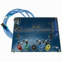
Manufacturer Part Number
CDB5534U
Description
EVAL BOARD FOR CS5534
Manufacturer
Cirrus Logic Inc
Specifications of CDB5534U
Number Of Adc's
1
Number Of Bits
24
Sampling Rate (per Second)
3.84k
Data Interface
Serial
Inputs Per Adc
2 Single
Input Range
0 ~ 2.5 V
Power (typ) @ Conditions
35mW @ 5 V
Voltage Supply Source
Analog and Digital, Dual ±
Operating Temperature
-40°C ~ 85°C
Utilized Ic / Part
CS5534
Description/function
Audio DSPs
Operating Supply Voltage
5 V
Product
Audio Modules
For Use With/related Products
C8051F320
Lead Free Status / RoHS Status
Contains lead / RoHS non-compliant
Lead Free Status / RoHS Status
Lead free / RoHS Compliant, Contains lead / RoHS non-compliant
Other names
598-1016


offset calibration on physical channel 2 and SDO
falls to indicate that the calibration is complete. To
perform additional calibrations, more commands
must be issued.
Note:
2.7. Using Multiple ADCs Synchronously
Some applications require synchronous data out-
puts from multiple ADCs converting different ana-
log channels. Multiple CS5531/32/33/34 parts can
be synchronized in a single system by using the fol-
lowing guidelines:
1) All of the ADCs in the system must be operated
from the same oscillator source.
2) All of the ADCs in the system must share com-
mon SCLK and SDI lines.
3) A software reset must be performed at the same
time for all of the ADCs after system power-up (by
selecting all of the ADCs using their respective CS
pins, and writing the reset sequence to all parts, us-
ing SDI and SCLK).
4) A start conversion command must be sent to all
of the ADCs in the system at the same time. The ±8
clock cycles of ambiguity for the first conversion
(or for a single conversion) will be the same for all
ADCs, provided that they were all reset at the same
time.
5) Conversions can be obtained by monitoring
SDO on only one ADC, (bring CS high for all but
one part) and reading the data out of each part indi-
vidually, before the next conversion data words are
ready.
36
The CSRs need not be written. If they are not
initialized, all the Setups point to their default
settings irrespective of the conversion or
calibration mode (i.e conversions can be
performed, but only physical channel 1 will be
converted). Further note that filter
convolutions are reset (i.e. flushed) if
consecutive conversions are performed on
two different physical channels. If
consecutive conversions are performed on
the same physical channel, the filter is not
reset. This allows the ADCs to more quickly
settle full-scale step inputs.
An example of a synchronous system using two
CS5532 parts is shown in Figure 15.
2.8. Conversion Output Coding
The CS5531/33 output 16-bit data conversion
words and the CS5532/34 output 24-bit data con-
version words. To read a conversion word the user
must read the conversion data register. The conver-
sion data register is 32 bits long and outputs the
conversions MSB first. The last byte of the conver-
sion data register contains data monitoring flags.
The channel indicator (CI) bits keep track of which
physical channel was converted and the overrange
flag (OF) monitors to determine if a valid conver-
sion was performed. Refer to the Conversion Data
Output Descriptions section for more details.
The CS5531/32/33/34 output data conversions in
binary format when operating in unipolar mode and
in two's complement format when operating in bi-
polar mode. Tables 4 and 5 show the code mapping
for both unipolar and bipolar mode. VFS in the ta-
bles refers to the positive full-scale voltage range of
the converter in the specified gain range, and -VFS
refers to the negative full-scale voltage range of the
converter. The total differential input range (be-
tween AIN+ and AIN-) is from 0 to VFS in unipo-
lar mode, and from -VFS to VFS in bipolar mode.
Figure 15. Synchronizing Multiple ADCs
CS5532
CS5532
OSC2
OSC2
SCLK
SCLK
SDO
SDO
SDI
CS
SDI
CS
CS5531/32/33/34-AS
SOURCE
CLOCK
µC
DS289F5
Related parts for CDB5534U
Image
Part Number
Description
Manufacturer
Datasheet
Request
R

Part Number:
Description:
Development Kit
Manufacturer:
Cirrus Logic Inc
Datasheet:
Part Number:
Description:
Development Kit
Manufacturer:
Cirrus Logic Inc
Datasheet:


Part Number:
Description:
High-efficiency PFC + Fluorescent Lamp Driver Reference Design
Manufacturer:
Cirrus Logic Inc
Datasheet:
Part Number:
Description:
Development Kit
Manufacturer:
Cirrus Logic Inc
Datasheet:
Part Number:
Description:
Development Kit
Manufacturer:
Cirrus Logic Inc
Datasheet:

Part Number:
Description:
Development Kit
Manufacturer:
Cirrus Logic Inc
Datasheet:
Part Number:
Description:
Development Kit
Manufacturer:
Cirrus Logic Inc
Datasheet:
Part Number:
Description:
Development Kit
Manufacturer:
Cirrus Logic Inc
Datasheet:
Part Number:
Description:
Development Kit
Manufacturer:
Cirrus Logic Inc
Datasheet:

Part Number:
Description:
EVALUATION BOARD FOR CS8427
Manufacturer:
Cirrus Logic Inc
Datasheet:

Part Number:
Description:
BOARD EVAL FOR CS8416 RCVR
Manufacturer:
Cirrus Logic Inc
Datasheet:

Part Number:
Description:
EVALUATION BOARD FOR CS8420
Manufacturer:
Cirrus Logic Inc
Datasheet:

Part Number:
Description:
KIT DEVELOPMENT EP9315 ARM9
Manufacturer:
Cirrus Logic Inc
Datasheet:

Part Number:
Description:
KIT DEVELOPMENT EP9302 ARM9
Manufacturer:
Cirrus Logic Inc
Datasheet: