ADP1613-12-EVALZ Analog Devices Inc, ADP1613-12-EVALZ Datasheet - Page 4
ADP1613-12-EVALZ
Manufacturer Part Number
ADP1613-12-EVALZ
Description
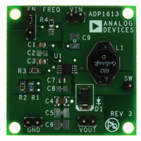
BOARD EVAL FOR ADP1613
Manufacturer
Analog Devices Inc
Specifications of ADP1613-12-EVALZ
Design Resources
Powering a 30V DAC from a 3V supply (CN0193)
Main Purpose
DC/DC, Step Up
Outputs And Type
1, Non-Isolated
Voltage - Output
12V
Current - Output
2A
Voltage - Input
2.5 ~ 5.5V
Regulator Topology
Boost
Board Type
Fully Populated
Utilized Ic / Part
ADP1613
Silicon Manufacturer
Analog Devices
Application Sub Type
Step Up DC/DC Converter
Kit Application Type
Power Management - Voltage Regulator
Silicon Core Number
ADP1613
Lead Free Status / RoHS Status
Lead free / RoHS Compliant
Power - Output
-
Frequency - Switching
-
Lead Free Status / RoHS Status
Lead free / RoHS Compliant, Lead free / RoHS Compliant


ADP1612/ADP1613
ABSOLUTE MAXIMUM RATINGS
Table 2.
Parameter
VIN, EN, FB to GND
FREQ to GND
COMP to GND
SS to GND
SW to GND
Operating Junction Temperature Range
Storage Temperature Range
Soldering Conditions
ESD (Electrostatic Discharge)
Stresses above those listed under Absolute Maximum Ratings
may cause permanent damage to the device. This is a stress
rating only; functional operation of the device at these or any
other conditions above those indicated in the operational
section of this specification is not implied. Exposure to absolute
maximum rating conditions for extended periods may affect
device reliability.
Absolute maximum ratings apply individually only, not in
combination.
Human Body Model
Rating
−0.3 V to +6 V
−0.3 V to V
1.0 V to 1.6 V
−0.3 V to +1.3 V
21 V
−40°C to +125°C
−65°C to +150°C
JEDEC J-STD-020
±5 kV
IN
+ 0.3 V
Rev. B | Page 4 of 28
THERMAL RESISTANCE
Junction-to-ambient thermal resistance (θ
specified for the worst-case conditions, that is, a device soldered
in a circuit board for surface-mount packages. The junction-to-
ambient thermal resistance is highly dependent on the application
and board layout. In applications where high maximum power
dissipation exists, attention to thermal board design is required.
The value of θ
and environmental conditions.
Table 3.
Package Type
8-Lead MSOP
1
BOUNDARY CONDITION
Modeled under natural convection cooling at 25°C ambient
temperature, JESD 51-7, and 1 W power input with 2- and
4-layer boards.
ESD CAUTION
Thermal numbers per JEDEC standard JESD 51-7.
2-Layer Board
4-Layer Board
JA
1
1
may vary, depending on PCB material, layout,
θ
206.9
162.2
JA
JA
θ
44.22
44.22
) of the package is
JC
Unit
°C/W
°C/W
Related parts for ADP1613-12-EVALZ
Image
Part Number
Description
Manufacturer
Datasheet
Request
R

Part Number:
Description:
EVAL BLANK ADISIMPOWER ADP1613
Manufacturer:
Analog Devices Inc
Datasheet:

Part Number:
Description:
650 kHz /1.3 MHz Step-Up PWM DC-to-DC Switching Converter with 2.0 A Current Limit
Manufacturer:
Analog Devices
Datasheet:

Part Number:
Description:
Blank SEPIC Demo Board
Manufacturer:
Analog Devices Inc
Datasheet:
Part Number:
Description:
Ank SEPIC-CUK Demo Board"
Manufacturer:
Analog Devices Inc
Datasheet:

Part Number:
Description:
±1.7g Dual-Axis IMEMS Accelerometer Evaluation Board
Manufacturer:
Analog Devices Inc
Datasheet:
Part Number:
Description:
Inertial Sensor Evaluation System
Manufacturer:
Analog Devices Inc
Datasheet:
Part Number:
Description:
Manufacturer:
Analog Devices Inc
Datasheet:
Part Number:
Description:
Manufacturer:
Analog Devices Inc
Datasheet:
Part Number:
Description:
Manufacturer:
Analog Devices Inc
Datasheet:
Part Number:
Description:
Manufacturer:
Analog Devices Inc
Datasheet:
Part Number:
Description:
Manufacturer:
Analog Devices Inc
Datasheet:
Part Number:
Description:
Manufacturer:
Analog Devices Inc
Datasheet:
Part Number:
Description:
Manufacturer:
Analog Devices Inc
Datasheet: