ADP2107-EVALZ Analog Devices Inc, ADP2107-EVALZ Datasheet - Page 7
ADP2107-EVALZ
Manufacturer Part Number
ADP2107-EVALZ
Description
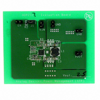
BOARD EVALUATION FOR ADP2107
Manufacturer
Analog Devices Inc
Specifications of ADP2107-EVALZ
Main Purpose
DC/DC, Step Down
Outputs And Type
1, Non-Isolated
Voltage - Output
2.5V
Current - Output
2A
Voltage - Input
2.7 ~ 5.5V
Regulator Topology
Buck
Frequency - Switching
1.2MHz
Board Type
Fully Populated
Utilized Ic / Part
ADP2107
Lead Free Status / RoHS Status
Lead free / RoHS Compliant
Power - Output
-


PIN CONFIGURATION AND FUNCTION DESCRIPTIONS
Table 4. Pin Function Descriptions
Pin No.
1
2, 3, 4, 15
5
6
7
8
9, 13
10, 12
11
14
16
EN
GND
COMP
SS
AGND
NC
PWIN2,
PWIN1
LX1, LX2
PGND
IN
FB
Mnemonic
Description
Enable Input. Drive EN high to turn on the device. Drive EN low to turn off the device and reduce the input
current to 0.1 μA.
Test Pins. These pins are used for internal testing and are not ground return pins. These pins are to be tied to the
AGND plane as close as possible to the ADP2105/ADP2106/ADP2107.
Feedback Loop Compensation Node. COMP is the output of the internal transconductance error amplifier. Place
a series RC network from COMP to AGND to compensate the converter. See the Loop Compensation section.
Soft Start Input. Place a capacitor from SS to AGND to set the soft start period. A 1 nF capacitor sets a 1 ms soft
start period.
Analog Ground. Connect the ground of the compensation components, the soft start capacitor, and the voltage
divider on the FB pin to the AGND pin as close as possible to the ADP2105/ ADP2106/ADP2107. The AGND is
also to be connected to the exposed pad of ADP2105/ADP2106/ADP2107.
No Connect. This is not internally connected and can be connected to other pins or left unconnected.
Power Source Inputs. The source of the PFET high-side switch. Bypass each PWIN pin to the nearest PGND plane with a
4.7 μF or greater capacitor as close as possible to the ADP2105/ADP2106/ ADP2107. See the Input Capacitor
Selection section.
Switch Outputs. The drain of the P-channel power switch and N-channel synchronous rectifier. These pins are to
be tied together and connected to the output LC filter between LX and the output voltage.
Power Ground. Connect the ground return of all input and output capacitors to the PGND pin using a power
ground plane as close as possible to the ADP2105/ADP2106/ADP2107. The PGND is then to be connected to the
exposed pad of the ADP2105/ADP2106/ADP2107.
Power Input. The power source for the ADP2105/ADP2106/ADP2107 internal circuitry. Connect IN and PWIN1
with a 10 Ω resistor as close as possible to the ADP2105/ADP2106/ADP2107. Bypass IN to AGND with a 0.1 μF or
greater capacitor. See the Input Filter section.
Output Voltage Sense or Feedback Input. For fixed output versions, connect to the output voltage. For
adjustable versions, FB is the input to the error amplifier. Drive FB through a resistive voltage divider to set the
output voltage. The FB regulation voltage is 0.8 V.
Figure 4. Pin Configuration
NC = NO CONNECT
Rev. C | Page 7 of 36
ADP2105/
ADP2106/
ADP2107
(Not to Scale)
TOP VIEW
PIN 1
INDICATOR
12 LX2
11 PGND
10 LX1
9
PWIN2
ADP2105/ADP2106/ADP2107
Related parts for ADP2107-EVALZ
Image
Part Number
Description
Manufacturer
Datasheet
Request
R

Part Number:
Description:
BOARD EVAL FOR ADP2107-1.8
Manufacturer:
Analog Devices Inc
Datasheet:
Part Number:
Description:
Blank ADISimPower Eval ADP2107
Manufacturer:
Analog Devices Inc
Datasheet:
Part Number:
Description:
BOARD EVAL FOR ADP2107ACPZ-1.8
Manufacturer:
Analog Devices Inc
Datasheet:

Part Number:
Description:
±1.7g Dual-Axis IMEMS Accelerometer Evaluation Board
Manufacturer:
Analog Devices Inc
Datasheet:
Part Number:
Description:
Inertial Sensor Evaluation System
Manufacturer:
Analog Devices Inc
Datasheet:
Part Number:
Description:
Manufacturer:
Analog Devices Inc
Datasheet:
Part Number:
Description:
Manufacturer:
Analog Devices Inc
Datasheet:
Part Number:
Description:
Manufacturer:
Analog Devices Inc
Datasheet:
Part Number:
Description:
Manufacturer:
Analog Devices Inc
Datasheet:
Part Number:
Description:
Manufacturer:
Analog Devices Inc
Datasheet:
Part Number:
Description:
Manufacturer:
Analog Devices Inc
Datasheet:
Part Number:
Description:
Manufacturer:
Analog Devices Inc
Datasheet:
Part Number:
Description:
Manufacturer:
Analog Devices Inc
Datasheet: