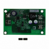
ADP1822-EVAL Analog Devices Inc, ADP1822-EVAL Datasheet

ADP1822-EVAL
Specifications of ADP1822-EVAL
Related parts for ADP1822-EVAL
ADP1822-EVAL Summary of contents
Page 1
... GENERAL DESCRIPTION The ADP1822 is a versatile and inexpensive synchronous buck PWM controller. The converter power input voltage range while the ADP1822 controller is specified from 3 5.5 V. The ADP1822 free-running frequency is logic- selectable at either 300 kHz or 600 kHz. Alternatively, it can be synchronized to an external clock at any frequency between 300 kHz and 1 ...
Page 2
... EVAL-ADP1822 TABLE OF CONTENTS Introduction ...................................................................................... 1 General Description ......................................................................... 1 Specifications..................................................................................... 1 Revision History ............................................................................... 2 Test Instructions ............................................................................... 3 Component Selection....................................................................... 4 Input Capacitor............................................................................. 4 Output Inductor ........................................................................... 4 Output Capacitor.......................................................................... 4 MOSFET Selection....................................................................... 4 Output Voltage.............................................................................. 5 Current Limit Set Resistor........................................................... 5 Setting the Soft Start..................................................................... 5 REVISION HISTORY 11/06—Revision 0: Initial Version Output Voltage Tracking ..............................................................5 Output Voltage Margining ...........................................................6 Control Loop Design and Equations ...
Page 3
... Table 3. Margining Description MAR MSEL Low (Jumper 3 X open) High (Jumper 3 High (Jumper 4 shorted) open) High (Jumper 3 Low (Jumper 4 shorted) shorted) Rev Page EVAL-ADP1822 Default Status Open Open Open Open Voltage Margin None High margin (FB connected to MUP) Low margin (FB connected to MDN) ...
Page 4
... EVAL-ADP1822 COMPONENT SELECTION INPUT CAPACITOR In continuous mode, the source current of the high-side MOSFET is a square wave of duty cycle V large voltage transients, use a low ESR input capacitor sized for the maximum rms current. The maximum rms capacitor current is given by I √D(1 − D) ...
Page 5
... L DSON _ low ⎠ 2 the regulation voltage, the output voltage regulates the desired voltage set by the voltage divider μA. CSL Rev Page EVAL-ADP1822 . A +42 μA current source at the ADP1822 DSON can be calculated from the following CSL Δ ⎛ ⎞ ⎜ ⎟ ...
Page 6
... EVAL-ADP1822 OUTPUT VOLTAGE MARGINING The ADP1822 features output voltage margining. MSEL is the margin select input. Drive MSEL high to activate the voltage margining feature. Drive MSEL low to regulate the output voltage to the nominal value. If not used, connect MSEL to GND. MAR is the margin control input. MAR is used with MSEL to control output voltage margining ...
Page 7
... CONTROL LOOP DESIGN AND EQUATIONS Figure simplified schematic diagram of the overall control loop. POWER STAGE TRANSFER FUNCTION The power stage transfer function of the ADP1822 is given by the following equation OUT × × × ω ω where ω ⋅ ω × the ESR of the output capacitor. ...
Page 8
... RAMP where V is the PWM peak ramp voltage (typically 1. RAMP the ADP1822 controller. Use the following guidelines to select the compensation components: 1. Set the loop gain cross frequency f (17) place the cross frequency f 2. Cancel ESR zero f by compensator pole Place the high frequency pole f attenuation of switching ripple and high frequency noise ...
Page 9
... Channel 1: Output Voltage (AC-Coupled), Channel 3: Output Current T Δ: 1.32mV @: 1.78mV A CH3 1.86V Channel 2: MAR Pin (Blue Trace), Channel 3: MSEL Pin (Pink Trace), Channel Rev Page EVAL-ADP1822 T Δ: 20.0mV @: –9.20mV 1 CH1 20.0mV M4.00µs A CH1 T 42.80% Figure 7. Output Voltage Ripple,10 A, Channel 1: Output Voltage ...
Page 10
... EVAL-ADP1822 CH2 2.00V M1.00ms CH3 2.00V CH4 100mV T 29.80% Figure 10. Output Voltage Margin Down, Channel 2: MAR Pin, Channel 3: MSEL Pin, Channel 4: Output Voltage 100 GAIN 20 0 –20 PHASE –40 –60 10 100 1k 10k FREQUENCY (Hz) Figure 11. Control Loop, Cross Frequency: 35.4 kHz, Phase Margin: 63.1° ...
Page 11
... To keep the inductance down, the traces from the high- side MOSFET and the low-side MOSFET to the DH and DL pins of the ADP1822, respectively, need to be relatively short and wide. 3. Place the source of Q1 and the drain of Q2 very close to each other to minimize inductance. Use a wide copper trace for this connection ...
Page 12
... VCC 7 18 TRKN MUP 8 17 TRKP MDN 16 9 SHDN MSEL 10 15 PWGD COMP 11 14 DGND GND SS R17 10kΩ ADP1822 J2 5% DGND AGND C12 22nF V OUT 16V C20 1nF 16V 1 TRKN Figure 13. Typical Application Schematic Diagram Rev Page OUT 3 CON4 C10 1 22µ ...
Page 13
... Figure 14. Top Layer Figure 15. Bottom Layer Figure 16. Silkscreen Top Rev Page EVAL-ADP1822 ...
Page 14
... EVAL-ADP1822 ORDERING INFORMATION BILL OF MATERIALS Table 5. Bill of Materials for ADP1822 Typical Application Circuit ( 1 Item Description 1 Capacitor, OS-CON, 180 μ mΩ × × Capacitor, Ceramic, 10 μ X5R,1206 3 Capacitor, Ceramic, 1 μ X5R, 0603 4 Capacitor, Ceramic, 1 μ X5R, 0603 5 Capacitor, OS-CON, 680 μ mΩ × ...
Page 15
... ORDERING GUIDE Model ADP1822-EVAL ESD CAUTION Package Description Evaluation Board Rev Page EVAL-ADP1822 ...
Page 16
... EVAL-ADP1822 NOTES ©2006 Analog Devices, Inc. All rights reserved. Trademarks and registered trademarks are the property of their respective owners. EB06388-0-11/06(0) Rev Page ...


