ADP1822-EVAL Analog Devices Inc, ADP1822-EVAL Datasheet - Page 4
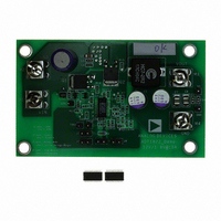
ADP1822-EVAL
Manufacturer Part Number
ADP1822-EVAL
Description
BOARD EVALUATION FOR ADP1822
Manufacturer
Analog Devices Inc
Datasheet
1.ADP1822-EVAL.pdf
(16 pages)
Specifications of ADP1822-EVAL
Main Purpose
DC/DC, Step Down
Outputs And Type
1, Non-Isolated
Voltage - Output
1.8V
Current - Output
10A
Voltage - Input
9 ~ 15V
Regulator Topology
Buck
Frequency - Switching
300kHz
Board Type
Fully Populated
Utilized Ic / Part
ADP1822
Lead Free Status / RoHS Status
Contains lead / RoHS non-compliant
Power - Output
-


EVAL-ADP1822
COMPONENT SELECTION
INPUT CAPACITOR
In continuous mode, the source current of the high-side
MOSFET is a square wave of duty cycle V
large voltage transients, use a low ESR input capacitor sized for
the maximum rms current. The maximum rms capacitor
current is given by I
OUTPUT INDUCTOR
In high switching applications, if the inductor is too big, the
dI/dt is too low and cannot respond to load changes quickly. If
the inductor is too small, the output ripple would be high.
Therefore, if good transient response is needed, smaller
inductors and larger capacitors are better, within the constraint
of the maximum allowed ripple current in the capacitor and the
maximum dissipation of the core (core temperature).
The output inductor can be chosen according to the following
equation:
where:
V
I
K
f
D is the duty cycle
Generally, K
OUTPUT CAPACITOR
The selection of C
capacitance. The output voltage ripple can be approximated as
Generally, the voltage ripple caused by the capacitance or ESR
depends on the capacitor chosen.
ESR affects the output voltage ripple; thus, an MLCC capacitor
is recommended because of its low ESR.
During a load transient on the output, the amount of
capacitance needed is determined by the maximum energy
stored in the inductor. The capacitance must be sufficient to
absorb the change in inductor current when a high current to
low current transition occurs and to supply the load when a low
current to high current transition occurs.
SW
OUT
OUT
CR
is the switching frequency.
is the ratio of current ripple, ΔI
is the rated output current.
is the output voltage.
C
L
Δ
V
OUT,
=
OUT
I
min1
OUT
cr
=
V
should be chosen around 20% ~ 40%.
K
OUT
Δ
=
CR
I
L
2
OUT
V
⎛
⎜
⎜
⎝
Δ
f
L
OUT
SW
ESR
I
√D(1 − D)
OUT
is determined by the ESR and the
1 (
Δ
−
+
2
V
L
D
up
8
)
f
SW
1
C
OUT
L
/I
O
⎞
⎟
⎟
⎠
.
OUT
/V
IN
. To prevent
Rev. 0 | Page 4 of 16
(1)
(2)
(3)
where:
ΔI
ΔV
stepped down.
ΔV
stepped up.
V
C
voltage ΔV
C
voltage ΔV
Select an output capacitance that is greater than both C
and C
Make sure that the ripple current rating of the output capacitors
is greater than the following current:
MOSFET SELECTION
The choice of MOSFET directly affects the dc-to-dc converter
performance. The MOSFET must have low on resistance
(R
reduce switching loss.
For the low-side (synchronous) MOSFET, the dominant loss is
the conduction loss. It can be calculated as
The gate charge loss is approximated by the following equation:
where:
V
Q
The high-side (switching) MOSFET has to be able to handle
conduction loss and switching loss. The high-side MOSFET
switching loss is approximated by the equation
where t
OUT,min1
OUT,min2
IN
G
G
DSON
OUT
up
down
is the driver voltage.
is the MOSFET total gate charge.
is the input voltage.
C
P
P
is the output voltage overshoot when the load is
I
P =
is the step load.
OUT, min2
COUT
) to reduce the conduction loss, and low gate charge to
C
G
T
OUT,
is the output voltage overshoot when the load is
R
,
low
is the minimum capacitance according to the overshoot
is the minimum capacitance according to the overshoot
=
and t
min2
V
up.
down.
V
=
=
G
.
IN
1 (
Q
F
=
I
are the rise and fall times of the MOSFET.
G
Δ
−
L
12
( 2
I
f
(
D
t
SW
L
V
R
2
)
2
IN
⎛
⎜ ⎜
⎝
+
I
−
t
O
Δ
F
UT
V
I
)
OUT
O
2
f
SW
UT
+
2
)
L
Δ
Δ
12
I
V
L
down
2
⎞
⎟ ⎟
⎠
R
DSON
OUT, min1
(4)
(5)
(6)
(7)
(8)
Related parts for ADP1822-EVAL
Image
Part Number
Description
Manufacturer
Datasheet
Request
R

Part Number:
Description:
216-02F-02imPower Eval ADP1822
Manufacturer:
Analog Devices Inc
Datasheet:
Part Number:
Description:
Blank ADISimPower Eval ADP1822
Manufacturer:
Analog Devices Inc
Datasheet:

Part Number:
Description:
±1.7g Dual-Axis IMEMS Accelerometer Evaluation Board
Manufacturer:
Analog Devices Inc
Datasheet:
Part Number:
Description:
Inertial Sensor Evaluation System
Manufacturer:
Analog Devices Inc
Datasheet:
Part Number:
Description:
Manufacturer:
Analog Devices Inc
Datasheet:
Part Number:
Description:
Manufacturer:
Analog Devices Inc
Datasheet:
Part Number:
Description:
Manufacturer:
Analog Devices Inc
Datasheet:
Part Number:
Description:
Manufacturer:
Analog Devices Inc
Datasheet:
Part Number:
Description:
Manufacturer:
Analog Devices Inc
Datasheet:
Part Number:
Description:
Manufacturer:
Analog Devices Inc
Datasheet:
Part Number:
Description:
Manufacturer:
Analog Devices Inc
Datasheet:
Part Number:
Description:
Manufacturer:
Analog Devices Inc
Datasheet:
Part Number:
Description:
Manufacturer:
Analog Devices Inc
Datasheet: