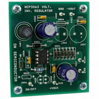
NCP3063DIPINVEVB ON Semiconductor, NCP3063DIPINVEVB Datasheet
NCP3063DIPINVEVB
Specifications of NCP3063DIPINVEVB


Related parts for NCP3063DIPINVEVB


NCP3063DIPINVEVB Summary of contents
Page 1
NCP3063, NCP3063B, NCV3063 1.5 A, Step-Up/Down/ Inverting Switching Regulators The NCP3063 Series is a higher frequency upgrade to the popular MC34063A and MC33063A monolithic DC−DC converters. These devices consist of an internal temperature compensated reference, comparator, a controlled duty cycle ...
Page 2
Switch Collector 8 Switch Emitter 2 7 Timing Capacitor 3 6 GND 4 5 (Top View) Figure 2. Pin Connections 8 N.C. COMPARATOR 7 I Sense Comparator Inverting Input N.C. Switch Collector I Sense ...
Page 3
PIN DESCRIPTION Pin No. Pin Name 1 Switch Collector Internal Darlington switch collector 2 Switch Emitter Internal Darlington switch emitter 3 Timing Capacitor Timing Capacitor Oscillator Input 4 GND Ground pin for all internal circuits 5 Comparator Inverting input pin ...
Page 4
ELECTRICAL CHARACTERISTICS Symbol Characteristic OSCILLATOR f Frequency OSC I / Discharge to Charge Current Ratio DISCHG I CHG I Capacitor Discharging Current DISCHG I Capacitor Charging Current CHG V Current Limit Sense Voltage IPK(Sense) OUTPUT SWITCH (Note 7) V Darlington ...
Page 5
Ct, CAPACITANCE (nF) Figure 5. Oscillator Frequency vs. Oscillator Timing Capacitor 2.4 2.2 ...
Page 6
T , JUNCTION TEMPERATURE (°C) J Figure 11. Comparator Threshold Voltage vs. Temperature 6.0 5.5 5.0 4.5 4.0 3.5 3.0 2.5 2.0 3.0 Figure 13. Standby ...
Page 7
The NCP3063 is a monolithic power switching regulator optimized for converter applications. The combination of its features enables the system designer to directly implement step−up, step−down, and voltage− inverting converters with a minimum number of external components. ...
Page 8
Peak Current Sense Comparator With a voltage ripple gated converter operating under normal conditions, output switch conduction is initiated by the Voltage Feedback comparator and terminated by the oscillator. Abnormal operating conditions occur when the converter output is overloaded or ...
Page 9
Notes 9, 10, 11) Step−Down out ) off SWCE * V out off out L(avg (Switch) I ...
Page 10
R201 0R15 + J201 + C201 C202 220 0.1 mF J202 1 GND Figure 16. Typical Buck Application Schematic Value of Components Name Value L201 47 mH, I > 1.5 A ...
Page 11
R101 0R15 + J101 + C101 C102 470 0.1 mF J102 1 GND Figure 19. Typical Boost Application Schematic Value of Components Name Value L101 100 mH, I > 1.5 A ...
Page 12
R501 0R15 + J501 + C501 C502 330 0.1 mF J502 1 GND Figure 22. Typical Voltage Inverting Application Schematic Value of Components Name Value L501 22 mH, I > 1.5 ...
Page 13
... Figure 25. The driving circuit is controlled from SWE Pin of the NCP3063 through frequency compensated resistor divider R7/R8. The driver IC2 is ON Semiconductor low cost dual NPN/PNP transistor BC846BPD. Its NPN transistor is connected as a super diode for charging the gate capacitance. The PNP transistor works as an emitter follower for discharging the gate capacitor ...
Page 14
− 50m IN IC1 NCP3063 8 N. COMP 100n 330m 0V Figure 27. Typical Buck Application Schematic with External PMOS Transistor ...
Page 15
... NSS35200, ON Semiconductor will be ideal for applications with 1 A output current, the input voltages and operating frequency 100 − 150 kHz. The switching speed could be improved by using desaturation diode D2. ...
Page 16
R1 IC1 NCP3063 8 N. COMP Figure 31. Typical Schematic of Buck Converter with RC Snubber and Pulse Feedback In some cases where there are oscillations on the output ...
Page 17
... G C SEATING PLANE −Z− 0.25 (0.010 *For additional information on our Pb−Free strategy and soldering details, please download the ON Semiconductor Soldering and Mounting Techniques Reference Manual, SOLDERRM/D. PACKAGE DIMENSIONS SOIC−8 NB CASE 751−07 ISSUE 0.10 (0.004 SOLDERING FOOTPRINT* 1 ...
Page 18
F −A− NOTE 2 C −T− N SEATING PLANE 0.13 (0.005) M PACKAGE DIMENSIONS 8 LEAD PDIP CASE 626−05 ISSUE http://onsemi.com 18 ...
Page 19
... NOTE 3 0.05 C *For additional information on our Pb−Free strategy and soldering details, please download the ON Semiconductor Soldering and Mounting Techniques Reference Manual, SOLDERRM/D. N. American Technical Support: 800−282−9855 Toll Free USA/Canada Europe, Middle East and Africa Technical Support: Phone: 421 33 790 2910 Japan Customer Focus Center Phone: 81− ...