NCP3063DIPINVEVB ON Semiconductor, NCP3063DIPINVEVB Datasheet - Page 15
NCP3063DIPINVEVB
Manufacturer Part Number
NCP3063DIPINVEVB
Description
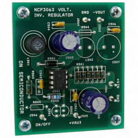
EVAL BOARD FOR NCP3063DIPINV
Manufacturer
ON Semiconductor
Specifications of NCP3063DIPINVEVB
Design Resources
NCP3063DIPINVEVB BOM NCP3063DIPINVEVB Gerbers NCP3063 EVB Schematic
Main Purpose
DC/DC, Negative Inverter
Outputs And Type
1, Non-Isolated
Voltage - Output
-12V
Voltage - Input
4.5 ~ 6 V
Regulator Topology
Inverting
Frequency - Switching
250kHz
Board Type
Fully Populated
Utilized Ic / Part
NCP3063
Lead Free Status / RoHS Status
Lead free / RoHS Compliant
Current - Output
-
Power - Output
-
Lead Free Status / Rohs Status
Lead free / RoHS Compliant
For Use With/related Products
NCP3063DIPINV
Other names
NCP3063DIPINVEVBOS


Figure 30. NCP3063 Efficiency vs. Output Current for
100
95
90
85
80
75
70
65
60
55
50
External Low V
0V
V
100m
0
IN
C1
= 8 − 19 V
0.1
+
Figure 29. Typical Buck Application Schematic with External Low V
0.2
C2
100n
150m
R1
CE(sat)
0.3
OUTPUT LOAD (Adc)
T
A
0.4
at V
= 255C
8
7
6
5
R2
1k
in
R3
0.5
IC1 NCP3063
N.C.
COMP
I
V
PK
= +5 V, f = 160 kHz,
CC
R4
33
0.6
SWC
SWE
1k7
GND
TC
0.7
Q1
1
2
3
4
0.8
http://onsemi.com
0.9
NSR0130
NSS35200
1
D2
C3
2n2
15
bipolar transistor is shown in the Figure 29. It is an ideal
solution for configurations where the input and output
voltage difference is small and high efficiency is required.
NSS35200,
ON Semiconductor will be ideal for applications with 1 A
output current, the input voltages up to 15 V and operating
frequency 100 − 150 kHz. The switching speed could be
improved by using desaturation diode D2.
Typical application of the buck converter with external
D1
1N5819
the
L1
CE
R5
low
33
(sat) PNP Transistor
33m
V
CE
(
sat)
100n
C5
transistor
V
OUT
100m
C6
= 3V3/1 A
+
GND
from
Related parts for NCP3063DIPINVEVB
Image
Part Number
Description
Manufacturer
Datasheet
Request
R

Part Number:
Description:
1.5 A, Step−Up/Down/Inverting Switching Regulators
Manufacturer:
ONSEMI [ON Semiconductor]
Datasheet:

Part Number:
Description:
EVAL BOARD FOR NCP3063DFBSTG
Manufacturer:
ON Semiconductor
Datasheet:

Part Number:
Description:
EVAL BOARD FOR NCP3063DIPBCK
Manufacturer:
ON Semiconductor
Datasheet:

Part Number:
Description:
EVAL BOARD FOR NCP3063SMDBST
Manufacturer:
ON Semiconductor
Datasheet:

Part Number:
Description:
EVAL BOARD FOR NCP3063SMINVG
Manufacturer:
ON Semiconductor
Datasheet:

Part Number:
Description:
EVAL BOARD FOR NCP3063BSTEXG
Manufacturer:
ON Semiconductor
Datasheet:

Part Number:
Description:
ON Semiconductor [VOLTAGE REGULATOR]
Manufacturer:
ON Semiconductor
Datasheet:
Part Number:
Description:
357-036-542-201 CARDEDGE 36POS DL .156 BLK LOPRO
Manufacturer:
ON Semiconductor
Datasheet:
Part Number:
Description:
357-036-542-201 CARDEDGE 36POS DL .156 BLK LOPRO
Manufacturer:
ON Semiconductor
Datasheet:
Part Number:
Description:
357-036-542-201 CARDEDGE 36POS DL .156 BLK LOPRO
Manufacturer:
ON Semiconductor
Datasheet:
Part Number:
Description:
357-036-542-201 CARDEDGE 36POS DL .156 BLK LOPRO
Manufacturer:
ON Semiconductor
Datasheet:
Part Number:
Description:
357-036-542-201 CARDEDGE 36POS DL .156 BLK LOPRO
Manufacturer:
ON Semiconductor
Datasheet:
Part Number:
Description:
357-036-542-201 CARDEDGE 36POS DL .156 BLK LOPRO
Manufacturer:
ON Semiconductor
Datasheet:
Part Number:
Description:
357-036-542-201 CARDEDGE 36POS DL .156 BLK LOPRO
Manufacturer:
ON Semiconductor
Datasheet:
Part Number:
Description:
357-036-542-201 CARDEDGE 36POS DL .156 BLK LOPRO
Manufacturer:
ON Semiconductor
Datasheet: