NCP1203GEVB ON Semiconductor, NCP1203GEVB Datasheet - Page 14
NCP1203GEVB
Manufacturer Part Number
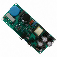
NCP1203GEVB
Description
EVAL BOARD FOR NCP1203G
Manufacturer
ON Semiconductor
Specifications of NCP1203GEVB
Design Resources
NCP1203GEVB BOM NCP1203GEVB Gerber Files NCP1203 EVB Schematic
Main Purpose
AC/DC, Primary Side
Outputs And Type
1, Isolated
Voltage - Output
19V
Current - Output
4A
Voltage - Input
85 ~ 230VAC
Regulator Topology
Flyback
Frequency - Switching
60kHz
Board Type
Fully Populated
Utilized Ic / Part
NPC1200
Lead Free Status / RoHS Status
Lead free / RoHS Compliant
Power - Output
-
Lead Free Status / Rohs Status
Lead free / RoHS Compliant
For Use With/related Products
NCP1203G
Other names
NCP1203GEVBOS


withstand accidental avalanche energy, e.g. during a
high−voltage spike superimposed over the mains, without
the help of a clamping network. If this leakage path
permanently forces a drain−source voltage above the
MOSFET BVdss (600 V), a clamping network is mandatory
and must be built around Rclamp and Clamp. Dclamp shall
react extremely fast and can be a MUR160 type. To calculate
the component values, the following formulas will help you:
R
with:
V
between 40 V to 80 V above the reflected output voltage
when the supply is heavily loaded.
V
diode voltage drop
L
N: the Ns:Np conversion ratio
F
†For information on tape and reel specifications, including part orientation and tape sizes, please refer to our Tape and Reel Packaging
C
2 @ V
ORDERING INFORMATION
Specifications Brochure, BRD8011/D.
out
SW
clamp =
clamp
leak
clamp
NCP1200P40G
NCP1200D40R2G
NCP1200P60G
NCP1200D60R2G
NCP1200P100G
NCP1200D100R2G
If the leakage inductance is kept low, the MTD1N60E can
: the switching frequency
+ Vf: the regulated output voltage level + the secondary
: the primary leakage inductance
clamp
: the desired clamping level, must be selected to be
Device
+
V
@ (V
ripple
L
leak
clamp
@ Fsw @ R
V
@ Ip
clamp
* (V
2
@ Fsw
out
F
F
F
clamp
SW
SW
SW
) Vf sec) @ N)
= 100 kHz
Type
= 40 kHz
= 60 kHz
http://onsemi.com
1200P100
1200P40
1200P60
Marking
200D4
200D6
200D1
14
V
which will damp the leakage oscillations but also provide
more capacitance at the MOSFET’s turn−off. The peak
voltage at which the leakage forces the drain is calculated
by:
where C
at the MOSFET opening. Typical values for Rsnubber and
Csnubber in this 4W application could respectively be 1.5
kW and 47 pF. Further tweaking is nevertheless necessary to
tune the dissipated power versus standby power.
Available Documents
“Implementing the NCP1200 in Low−cost AC−DC
Converters”, AND8023/D.
“Conducted EMI Filter Design for the NCP1200’’,
AND8032/D.
“Ramp Compensation for the NCP1200’’, AND8029/D.
TRANSient and AC models available to download at:
http://onsemi.com/pub/NCP1200
NCP1200 design spreadsheet available to download at:
http://onsemi.com/pub/NCP1200
V
ripple
max
Another option lies in implementing a snubber network
: the clamping ripple, could be around 20 V
+ Ip @
lump
represents the total parasitic capacitance seen
(Pb−Free)
(Pb−Free)
(Pb−Free)
(Pb−Free)
(Pb−Free)
(Pb−Free)
Package
SOIC−8
SOIC−8
SOIC−8
PDIP−8
PDIP−8
PDIP−8
C
L
lump
leak
2500 / Tape & Reel
2500 / Tape & Reel
2500 / Tape & Reel
50 Units / Rail
50 Units / Rail
50 Units / Rail
Shipping
†
Related parts for NCP1203GEVB
Image
Part Number
Description
Manufacturer
Datasheet
Request
R

Part Number:
Description:
Current Mode Controller Fixed Frequency Operation
Manufacturer:
ON Semiconductor
Datasheet:
Part Number:
Description:
ON Semiconductor [VOLTAGE REGULATOR]
Manufacturer:
ON Semiconductor
Datasheet:
Part Number:
Description:
357-036-542-201 CARDEDGE 36POS DL .156 BLK LOPRO
Manufacturer:
ON Semiconductor
Datasheet:
Part Number:
Description:
357-036-542-201 CARDEDGE 36POS DL .156 BLK LOPRO
Manufacturer:
ON Semiconductor
Datasheet:
Part Number:
Description:
357-036-542-201 CARDEDGE 36POS DL .156 BLK LOPRO
Manufacturer:
ON Semiconductor
Datasheet:
Part Number:
Description:
357-036-542-201 CARDEDGE 36POS DL .156 BLK LOPRO
Manufacturer:
ON Semiconductor
Datasheet:
Part Number:
Description:
357-036-542-201 CARDEDGE 36POS DL .156 BLK LOPRO
Manufacturer:
ON Semiconductor
Datasheet:
Part Number:
Description:
357-036-542-201 CARDEDGE 36POS DL .156 BLK LOPRO
Manufacturer:
ON Semiconductor
Datasheet:
Part Number:
Description:
357-036-542-201 CARDEDGE 36POS DL .156 BLK LOPRO
Manufacturer:
ON Semiconductor
Datasheet:
Part Number:
Description:
357-036-542-201 CARDEDGE 36POS DL .156 BLK LOPRO
Manufacturer:
ON Semiconductor
Datasheet:
Part Number:
Description:
357-036-542-201 CARDEDGE 36POS DL .156 BLK LOPRO
Manufacturer:
ON Semiconductor
Datasheet:
Part Number:
Description:
357-036-542-201 CARDEDGE 36POS DL .156 BLK LOPRO
Manufacturer:
ON Semiconductor
Datasheet:
Part Number:
Description:
Manufacturer:
ON Semiconductor
Datasheet:
Part Number:
Description:
Manufacturer:
ON Semiconductor
Datasheet: