NCP1203GEVB ON Semiconductor, NCP1203GEVB Datasheet - Page 4
NCP1203GEVB
Manufacturer Part Number
NCP1203GEVB
Description
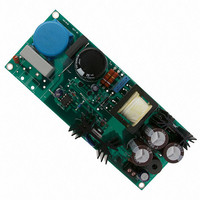
EVAL BOARD FOR NCP1203G
Manufacturer
ON Semiconductor
Specifications of NCP1203GEVB
Design Resources
NCP1203GEVB BOM NCP1203GEVB Gerber Files NCP1203 EVB Schematic
Main Purpose
AC/DC, Primary Side
Outputs And Type
1, Isolated
Voltage - Output
19V
Current - Output
4A
Voltage - Input
85 ~ 230VAC
Regulator Topology
Flyback
Frequency - Switching
60kHz
Board Type
Fully Populated
Utilized Ic / Part
NPC1200
Lead Free Status / RoHS Status
Lead free / RoHS Compliant
Power - Output
-
Lead Free Status / Rohs Status
Lead free / RoHS Compliant
For Use With/related Products
NCP1203G
Other names
NCP1203GEVBOS


1. Max value @ T
2. Max value @ T
ELECTRICAL CHARACTERISTICS
V
DYNAMIC SELF−SUPPLY (All Frequency Versions, Otherwise Noted)
INTERNAL CURRENT SOURCE
DRIVE OUTPUT
CURRENT COMPARATOR (Pin 5 Un−loaded)
INTERNAL OSCILLATOR (V
FEEDBACK SECTION (V
SKIP CYCLE GENERATION
V
V
V
Internal IC Consumption, No Output Load on Pin 5
Internal IC Consumption, 1 nF Output Load on Pin 5, F
Internal IC Consumption, 1 nF Output Load on Pin 5, F
Internal IC Consumption, 1 nF Output Load on Pin 5, F
Internal IC Consumption, Latchoff Phase
High−voltage Current Source, V
High−voltage Current Source, V
Output Voltage Rise−time @ CL = 1 nF, 10−90% of Output Signal
Output Voltage Fall−time @ CL = 1 nF, 10−90% of Output Signal
Source Resistance (drive = 0, Vgate = V
Sink Resistance (drive = 11 V, Vgate = 1 V)
Input Bias Current @ 1 V Input Level on Pin 3
Maximum internal Current Setpoint
Default Internal Current Setpoint for Skip Cycle Operation
Propagation Delay from Current Detection to Gate OFF State
Leading Edge Blanking Duration
Oscillation Frequency, 40 kHz Version
Oscillation Frequency, 60 kHz Version
Oscillation Frequency, 100 kHz Version
Built−in Frequency Jittering, F
Built−in Frequency Jittering, F
Built−in Frequency Jittering, F
Maximum Duty Cycle
Internal Pullup Resistor
Pin 3 to Current Setpoint Division Ratio
Default skip mode level
Pin 1 internal output impedance
CC
CC
CC
CC
= 11 V unless otherwise noted)
Increasing Level at Which the Current Source Turns−off
Decreasing Level at Which the Current Source Turns−on
Decreasing Level at Which the Latchoff Phase Ends
J
J
= −25°C.
= 25°C, please see characterization curves.
CC
= 11 V, Pin 5 Loaded by 1 kW)
CC
SW
SW
SW
= 11 V, Pin 5 Loaded by 1 kW)
CC
CC
= 40 kHz
= 60 kHz
= 100 kHz
= 10 V
= 0 V
Rating
CCHMAX
(For typical values T
− 1 V)
SW
SW
SW
http://onsemi.com
= 40 kHz
= 60 kHz
= 100 kHz
J
= +25°C, for min/max values T
4
Pin
6
6
6
6
6
6
6
6
8
8
5
5
5
5
3
3
3
3
3
−
−
−
−
−
−
−
2
−
1
1
Symbol
V
V
V
Dmax
Vskip
CClatch
CCOFF
I
T
T
Iratio
R
I
f
f
f
Zout
I
I
I
I
I
R
f
f
f
Rup
CCON
Lskip
CC1
CC2
CC2
CC2
CC3
Limit
OSC
OSC
OSC
I
I
jitter
jitter
jitter
I
DEL
LEB
C1
C2
T
T
OH
IB
OL
J
r
f
= −25°C to +125°C, Max T
10.3
Min
8.8
2.8
0.8
1.1
27
36
52
86
74
−
−
−
−
−
−
−
−
−
5
−
−
−
−
−
−
−
−
−
−
11.4
0.02
Typ
710
350
350
100
230
103
300
450
620
9.8
6.3
1.2
1.4
1.9
4.0
4.9
0.9
8.0
4.0
1.4
67
28
40
12
42
61
80
25
J
Note 1
Note 2
Note 2
Note 2
= 150°C,
Max
12.5
880
160
116
1.4
1.6
2.2
1.0
1.6
11
61
25
48
70
87
−
−
−
−
−
−
−
−
−
−
−
−
−
−
−
Hz/V
Hz/V
Hz/V
Unit
kHz
kHz
kHz
mA
mA
mA
mA
mA
mV
mA
mA
mA
kW
kW
ns
ns
ns
ns
W
W
%
V
V
V
V
V
−
Related parts for NCP1203GEVB
Image
Part Number
Description
Manufacturer
Datasheet
Request
R

Part Number:
Description:
Current Mode Controller Fixed Frequency Operation
Manufacturer:
ON Semiconductor
Datasheet:
Part Number:
Description:
ON Semiconductor [VOLTAGE REGULATOR]
Manufacturer:
ON Semiconductor
Datasheet:
Part Number:
Description:
357-036-542-201 CARDEDGE 36POS DL .156 BLK LOPRO
Manufacturer:
ON Semiconductor
Datasheet:
Part Number:
Description:
357-036-542-201 CARDEDGE 36POS DL .156 BLK LOPRO
Manufacturer:
ON Semiconductor
Datasheet:
Part Number:
Description:
357-036-542-201 CARDEDGE 36POS DL .156 BLK LOPRO
Manufacturer:
ON Semiconductor
Datasheet:
Part Number:
Description:
357-036-542-201 CARDEDGE 36POS DL .156 BLK LOPRO
Manufacturer:
ON Semiconductor
Datasheet:
Part Number:
Description:
357-036-542-201 CARDEDGE 36POS DL .156 BLK LOPRO
Manufacturer:
ON Semiconductor
Datasheet:
Part Number:
Description:
357-036-542-201 CARDEDGE 36POS DL .156 BLK LOPRO
Manufacturer:
ON Semiconductor
Datasheet:
Part Number:
Description:
357-036-542-201 CARDEDGE 36POS DL .156 BLK LOPRO
Manufacturer:
ON Semiconductor
Datasheet:
Part Number:
Description:
357-036-542-201 CARDEDGE 36POS DL .156 BLK LOPRO
Manufacturer:
ON Semiconductor
Datasheet:
Part Number:
Description:
357-036-542-201 CARDEDGE 36POS DL .156 BLK LOPRO
Manufacturer:
ON Semiconductor
Datasheet:
Part Number:
Description:
357-036-542-201 CARDEDGE 36POS DL .156 BLK LOPRO
Manufacturer:
ON Semiconductor
Datasheet:
Part Number:
Description:
Manufacturer:
ON Semiconductor
Datasheet:
Part Number:
Description:
Manufacturer:
ON Semiconductor
Datasheet: