STEVAL-ISA017V1 STMicroelectronics, STEVAL-ISA017V1 Datasheet - Page 4
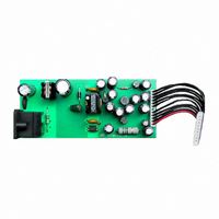
STEVAL-ISA017V1
Manufacturer Part Number
STEVAL-ISA017V1
Description
POWER SUPPLY FOR STB US-110V
Manufacturer
STMicroelectronics
Type
AC/DC Switching Convertersr
Specifications of STEVAL-ISA017V1
Mfg Application Notes
Quasi AppNote
Design Resources
STEVAL-ISA017V1 Gerber Files STEVAL-ISA017V1 Schematic STEVAL-ISA017V1 Bill of Materials
Main Purpose
AC/DC, Primary Side
Outputs And Type
6, Non-Isolated
Power - Output
17W
Voltage - Output
1.23V, 5V, 2.5V, 12V, 3.3V, 8V
Current - Output
1.7A, 1A, 700mA, 500mA, 450mA, 40mA
Voltage - Input
88 ~ 135VAC
Regulator Topology
Flyback
Board Type
Fully Populated
Utilized Ic / Part
L6565
Input Voltage
88 V to 138 V
Output Voltage
1.2 V to 12 V
Product
Power Management Modules
Lead Free Status / RoHS Status
Lead free / RoHS Compliant
Frequency - Switching
-
Lead Free Status / Rohs Status
Lead free / RoHS Compliant
For Use With/related Products
L6565
Other names
497-5680
Available stocks
Company
Part Number
Manufacturer
Quantity
Price


L6565
ELECTRICAL CHARACTERISTCS (continued)
(T
4/17
CURRENT SENSE COMPARATOR
ZERO CURRENT DETECTOR/ SYNCHRONIZATION
START TIMER
GATE DRIVER
Symbol
I
T
I
V
V
V
V
V
V
ZCDsnk
j
ZCDsrc
I
I
t
t
I
BLANK
I
START
COMP
V
ZCDb
V
d(H-L)
= -25 to 125°C, V
ZCDH
ZCDr
V
GDoff
COMP
CSdis
ZCDL
ZCDA
ZCDT
V
GB
I
G
CS
CSx
DIS
OH
t
t
OL
f
r
V
(1) Parameters guaranteed by design, not tested in production.
Voltage Gain
Gain-Bandwidth Product
Source Current
Sink Current
Upper Clamp Voltage
Lower Clamp Voltage
Input Bias Current
Delay to Output
Current Sense Reference Clamp
Hiccup-mode OCP level
Upper Clamp Voltage
Lower Clamp Voltage
Arming Voltage
(positive-going edge)
Triggering Voltage
(negative-going edge)
Input Bias Current
Source Current Capability
Sink Current Capability
Disable Threshold
Restart Current After Disable
Blanking time after pin 7 high-to-
low transition
Start Timer period
Dropout Voltage
Current Fall Time
Current Rise Time
I
GD
sink current
CC
Parameter
= 12V, C
o
= 1nF; unless otherwise specified)
Open loop
V
V
I
I
V
V
V
V
I
I
(1)
V
V
V
V
I
I
I
I
Vcc = 4 V, V
SOURCE
SINK
ZCD
ZCD
GDsource
GDsource
GDsink
GDsink
COMP
COMP
COMP
COMP
COMP
CS
ZCD
ZCD
COMP
COMP
= 0
= 3mA
= - 3mA
= 0.5 mA
= 1 to 4.5 V
< V
= Upper clamp, V
= Upper clamp, V
= 200mA
= 20mA
= Upper clamp, V
= 4V, V
= 4V, V
= 2.5 V
Test Condition
= 200mA
= 20mA
DIS
= 0.5 mA
3.2 V
GD
, Vcc > Vcc
INV
INV
= 1 V
= 2.4 V
= 2.6 V
VFF
VFF
VFF
off
= 1.5V
= 0V
= 3V
Min.
1.28
0.62
1.85
150
250
2.5
4.7
0.3
-70
60
-2
-3
5
3
5
-0.05
Typ.
2.25
0.65
-150
-3.5
200
200
400
4.5
5.5
1.4
0.7
2.0
5.2
2.1
1.6
3.5
1.2
0.7
80
18
40
40
10
1
0
2
Max.
2.55
0.78
-230
450
250
550
100
100
1.5
0.2
2.2
6.1
-10
0.3
10
-5
-1
1
2
1
2
MHz
Unit
mA
mA
mA
mA
mV
mA
dB
µA
µA
µA
ns
µs
µs
ns
ns
V
V
V
V
V
V
V
V
V
V
Related parts for STEVAL-ISA017V1
Image
Part Number
Description
Manufacturer
Datasheet
Request
R

Part Number:
Description:
BOARD RGB CTR ST7,STP08C596MTR
Manufacturer:
STMicroelectronics
Datasheet:

Part Number:
Description:
Power Management IC Development Tools Full Speed USB to RS232 Bridge Demo
Manufacturer:
STMicroelectronics
Datasheet:
Part Number:
Description:
Power Management IC Development Tools 2.5W solar eval BRD USB SPV1040 LD39050
Manufacturer:
STMicroelectronics
Datasheet:

Part Number:
Description:
BOARD EVAL FOR MEMS SENSORS
Manufacturer:
STMicroelectronics
Datasheet:

Part Number:
Description:
KIT DEV STARTER ST10F276Z5
Manufacturer:
STMicroelectronics
Datasheet:

Part Number:
Description:
BOARD EVAL HDMI $ VIDEO SWITCH
Manufacturer:
STMicroelectronics
Datasheet:

Part Number:
Description:
BOARD DEMO ACCELEROMETER DIL24
Manufacturer:
STMicroelectronics
Datasheet:

Part Number:
Description:
BOARD STLM75/STDS75/ST72F651
Manufacturer:
STMicroelectronics
Datasheet:

Part Number:
Description:
EVAL BOARD 3AXIS MEMS ACCELLRMTR
Manufacturer:
STMicroelectronics
Datasheet:

Part Number:
Description:
BOARD EVAL 8BIT MICRO + TDE1708
Manufacturer:
STMicroelectronics
Datasheet:
Part Number:
Description:
STMicroelectronics [RIPPLE-CARRY BINARY COUNTER/DIVIDERS]
Manufacturer:
STMicroelectronics
Datasheet:
Part Number:
Description:
STMicroelectronics [LIQUID-CRYSTAL DISPLAY DRIVERS]
Manufacturer:
STMicroelectronics
Datasheet:
Part Number:
Description:
BOARD EVAL FOR MEMS SENSORS
Manufacturer:
STMicroelectronics
Datasheet: