IRDC3820 International Rectifier, IRDC3820 Datasheet - Page 11
IRDC3820
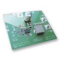
Manufacturer Part Number
IRDC3820
Description
BOARD EVAL SYNC BUCK CONVERTER
Manufacturer
International Rectifier
Specifications of IRDC3820
Silicon Manufacturer
International Rectifier
Kit Application Type
Power Management - Voltage Regulator
Application Sub Type
Synchronous Buck Converter
Features
Programmable Soft Start, Programmable
Rohs Compliant
Yes


Fig. 10: Typical application of the IR3820 for
Application Information
Design Example:
The following example is a typical application for
the IR3820. The application circuit is shown in
page 17.
Output Voltage Programming
Output voltage is programmed by reference
voltage and external voltage divider. The Fb pin
is the inverting input of the error amplifier, which
is internally referenced to 0.6V. The divider is
ratioed to provide 0.6V at the Fb pin when the
output is at its desired value. The output voltage
is defined by using the following equation:
When an external resistor divider is connected to
the output as shown in figure 10.
Equation (4) can be rewritten as:
For the calculated values of R
11/04/08
V
V
feedback compensation section.
I
F
ΔV
R
o
in
o
s
9
=
=
=
=
=
o
R
12
1
600
12
≤
8
programming the output voltage
8 .
∗
IR3624
V
A
IR3820
30
⎛
⎜ ⎜
⎝
V,(
o
V
V
=
kHz
V
O
V
−
mV
ref
V
ref
13
ref
∗
⎞
⎟ ⎟
⎠
Fb
⎛
⎜ ⎜
⎝
2 .
1
+
V,
--(
R
R
8
9
) 5
max
⎞
⎟ ⎟
⎠
--(
V
) 4
)
OUT
8
R
R
8
9
and R
9
see
Soft-Start Programming
The soft-start timing can be programmed by
selecting the soft-start capacitance value. The
start-up time of the converter can be calculated
by using:
Where T
For a start-up time of 11ms, the soft-start
capacitor will be 0.22uF.
Vc supply for single input voltage
To drive the high-side switch, it is necessary to
supply a gate voltage at least 4V greater than the
bus voltage. This is achieved by using a charge
pump configuration as shown in figure 11. This
method is simple and inexpensive. The operation
of the circuit is as follows: when the lower
MOSFET is turned on, the capacitor
pulled down to ground and charges, up to V
value, through the diode (D1). The bus voltage
will be added to this voltage when upper
MOSFET turns on in next cycle, and providing
supply voltage (Vc) through diode (D2). Vc is
approximately:
Capacitors in the range of 0.1uF are generally
adequate for most applications. The diodes must
be a fast recovery device to minimize the amount
of charge fed back from the charge pump
capacitor into V
to block the full power rail voltage, which is seen
when the high side MOSFET is switched on. For
low voltage application, schottky diodes can be
used to minimize forward drop across the diodes
at start up.
Fig. 11: Charge pump circuit to generate
V
start
C
≅
is the desired start-up time (ms)
2
∗
C
V
SS
BUS
bus
≅
−
. The diodes need to be able
Vc voltage
20
(
V
D
μ
IR3820MPbF
1
A
+
*
V
T
D
start
2
)
--(
--(
) 6
PD-60329
) 1
(C1) is
BUS
11
Related parts for IRDC3820
Image
Part Number
Description
Manufacturer
Datasheet
Request
R

Part Number:
Description:
SCHOTTKY RECTIFIER
Manufacturer:
International Rectifier Corp.
Datasheet:
Part Number:
Description:
SCHOTTKY RECTIFIER
Manufacturer:
International Rectifier Corp.
Datasheet:
Part Number:
Description:
SCHOTTKY RECTIFIER
Manufacturer:
International Rectifier Corp.
Datasheet:
Part Number:
Description:
SCHOTTKY RECTIFIER
Manufacturer:
International Rectifier Corp.
Datasheet:
Part Number:
Description:
SCHOTTKY RECTIFIER
Manufacturer:
International Rectifier Corp.
Datasheet:
Part Number:
Description:
SCHOTTKY RECTIFIER
Manufacturer:
International Rectifier Corp.
Datasheet:
Part Number:
Description:
SCHOTTKY RECTIFIER
Manufacturer:
International Rectifier Corp.
Datasheet:
Part Number:
Description:
SCHOTTKY RECTIFIER
Manufacturer:
International Rectifier Corp.
Datasheet:
Part Number:
Description:
SCHOTTKY RECTIFIER
Manufacturer:
International Rectifier Corp.
Datasheet:
Part Number:
Description:
SCHOTTKY RECTIFIER
Manufacturer:
International Rectifier Corp.
Datasheet:
Part Number:
Description:
SCHOTTKY RECTIFIER
Manufacturer:
International Rectifier Corp.
Datasheet:
Part Number:
Description:
SCHOTTKY RECTIFIER
Manufacturer:
International Rectifier Corp.
Datasheet:
Part Number:
Description:
SCHOTTKY RECTIFIER
Manufacturer:
International Rectifier Corp.
Datasheet:
Part Number:
Description:
SCHOTTKY RECTIFIER
Manufacturer:
International Rectifier Corp.
Datasheet:
Part Number:
Description:
SCHOTTKY RECTIFIER
Manufacturer:
International Rectifier Corp.
Datasheet: