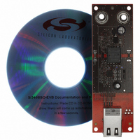
SI3400ISO-EVB Silicon Laboratories Inc, SI3400ISO-EVB Datasheet - Page 11

SI3400ISO-EVB
Manufacturer Part Number
SI3400ISO-EVB
Description
BOARD EVAL ISOLATED FOR SI3400
Manufacturer
Silicon Laboratories Inc
Type
PWM Controllersr
Datasheet
1.SI3400-E1-GM.pdf
(20 pages)
Specifications of SI3400ISO-EVB
Mfg Application Notes
SI3400/01 High Power AppNote Si3400/1 PoE PD Controllers AppNote
Main Purpose
Special Purpose DC/DC, Power Over Ethernet
Outputs And Type
1, Isolated
Voltage - Output
5V
Voltage - Input
44 ~ 57V
Regulator Topology
Flyback
Frequency - Switching
350kHz
Board Type
Fully Populated
Utilized Ic / Part
Si3400
Input Voltage
5 V
Output Voltage
3.3 V
Interface Type
Ethernet
Maximum Operating Temperature
+ 85 C
Minimum Operating Temperature
- 40 C
Product
Power Management Modules
For Use With/related Products
Si3400
Lead Free Status / RoHS Status
Contains lead / RoHS non-compliant
Current - Output
-
Power - Output
-
Lead Free Status / Rohs Status
Lead free / RoHS Compliant
Other names
336-1353
SI3400ISO-EVB
SI3400ISO-EVB
3.2.1. Rectification Diode Bridges and
The 802.3 specification defines the input voltage at the
RJ-45 connector of the PD with no reference to polarity.
In other words, the PD must be able to accept power of
either polarity at each of its inputs. This requirement
necessitates the use of two sets of diode bridges, one
for the CT1 and CT2 pins and one for the SP1 and SP2
pins to rectify the voltage. Furthermore, the standard
requires that a PD withstand a high-voltage transient
surge consisting of a 1000 V common-mode impulse
with 300 ns rise time and 50 µs half fall time. Typically,
the diode bridge and the surge suppressor have been
implemented externally, adding cost and complexity to
the PD system design.
The diode bridge* and the surge suppressor have been
integrated into the Si3400 and Si3401, thus reducing
system cost and design complexity.
*Note: Silicon Laboratories recommends that on-chip diode
By integrating the diode bridges, the Si3400 and Si3401
gain access to the input side of the diode bridge.
Monitoring the voltage at the input of the diode bridges
instead of the voltage across the load capacitor
provides the earliest indication of a power loss. This true
early power loss indicator, PLOSS, provides a local
microcontroller time to save states and shut down
gracefully before the load capacitor discharges below
the minimum 802.3-specified operating voltage of 36 V.
Integration
optimization of the clamping voltage and guarantees
protection of all connected circuitry.
Input Voltage (|CT1-
CT2| or |SP1-SP2|)
57 V down to 36 V
Surge Suppressor
42 V up to 57 V
bridges be bypassed when >10 W of output power is
required.
2.7 V to 11 V
Table 9. Hotswap Interface Modes
11 V to 14 V
14 V to 22 V
22 V to 42 V
0 V to 2.7 V
of
the
surge
Inactive
Detection signature
Detection turns off and
internal bias starts
Classification signature
Transition region
Switcher operating mode
(hysteresis limit based on
rising input voltage)
Switcher operating mode
(hysteresis limit based on
falling input voltage)
Si3400 and Si3401
suppressor
Mode
enables
Rev. 0.9
As an added benefit, the transient surge suppressor,
when tripped, actively disables the hotswap interface
and switching regulator, preventing downstream circuits
from encountering the high-energy transients.
3.2.2. Detection
In order to identify a device as a valid PD, a PSE will
apply a voltage in the range of 2.8 V to 10 V on the
cable and look for the 25.5 kΩ signature resistor. The
Si3400 and Si3401 will react to voltages in this range by
connecting an external 25.5 kΩ resistor between VPOS
and VNEG. This external resistor and internal low-
leakage control circuitry create the proper signature to
alert the PSE that a valid PD has been detected and is
ready to have power applied. The internal hotswap
switch is disabled during this time to prevent the
switching regulator and attached load circuitry from
generating errors in the detection signature.
Since the Si3400 and Si3401 integrate the diode
bridges, the IC can compensate for the voltage and
resistance effects of the diode bridges. The 802.3
specification requires that the PSE use a multi-point,
∆V/∆I measurement technique to remove the diode-
induced dc offset from the signature resistance
measurement. However, the specification does not
address the diode's nonlinear resistance and the error
induced in the signature resistor measurement. Since
the diode's resistance appears in series with the
signature resistor, the PD system must find some way of
compensating for this error. In systems where the diode
bridges are external, compensation is difficult and
suffers from errors. Since the diode bridges are
integrated in the Si3400 and Si3401, the IC can easily
compensate for this error by offsetting resistance across
all operating conditions and thus meeting the 802.3
requirements. An added benefit is that this function can
be tested during the IC’s automated testing step,
guaranteeing system compliance when used in the final
PD application. For more information about supporting
higher-power
“AN313: Using the Si3400 and Si3401 in High Power
Applications” and “AN314: Power Combining Circuit for
PoE for up to 18.5 W Output”.
3.2.3. Classification
Once the PSE has detected a valid PD, the PSE may
classify the PD for one of five power levels or classes. A
class is based on the expected power consumption of
the powered device. An external resistor sets the
nominal class current that can then be read by the PSE
to determine the proper power requirements of the PD.
When the PSE presents a fixed voltage between 15.5 V
and 20.5 V to the PD, the Si3400 and Si3401 assert the
class current from VPOS through the RCL resistor.
applications
Si3400/Si3401
(above
12.95 W),
see
11


