MCP4728EV Microchip Technology, MCP4728EV Datasheet - Page 37
MCP4728EV
Manufacturer Part Number
MCP4728EV
Description
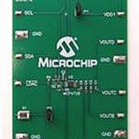
BOARD EVAL 12BIT 4CH DAC MCP4728
Manufacturer
Microchip Technology
Type
D/Ar
Specifications of MCP4728EV
Number Of Dac's
4
Number Of Bits
12
Outputs And Type
1, Single Ended
Data Interface
I²C
Settling Time
6µs
Dac Type
Voltage
Voltage Supply Source
Single
Operating Temperature
-40°C ~ 125°C
Utilized Ic / Part
MCP4728
Product
Data Conversion Development Tools
Resolution
12 bit
Interface Type
I2C
Supply Voltage (max)
5.5 V
Supply Voltage (min)
2.7 V
Silicon Manufacturer
Microchip
Silicon Core Number
MCP4728
Kit Application Type
Data Converter
Application Sub Type
DAC
Kit Contents
Board
For Use With/related Products
MCP4728
Lead Free Status / RoHS Status
Lead free / RoHS Compliant
Lead Free Status / RoHS Status
Lead free / RoHS Compliant, Lead free / RoHS Compliant
Available stocks
Company
Part Number
Manufacturer
Quantity
Price
Company:

Part Number:
MCP4728EV
Manufacturer:
Microchip Technology
Quantity:
135
Company:
Part Number:
MCP4728EV
Manufacturer:
MICROCHIP
Quantity:
12 000


5.6.5
When the device receives this command, it updates the
DAC voltage reference selection bit (V
channel. The EEPROM data is not affected by this
command. The affected channel’s analog output is
updated after the acknowledge pulse of the last byte.
Figure 5-12
for Select V
5.6.6
When the device receives this command, it updates the
Power-Down selection bits (PD1, PD0) of each
channel. The EEPROM data is not affected by this
command. The affected channel is updated after the
acknowledge pulse of the last byte.
an example of the write command for the Select
Power-Down bits.
5.6.7
When the device receives this command, it updates the
gain selection bits (G
data is not affected by this command. The analog
output is updated after the acknowledge pulse of the
last byte.
command for select gain bits.
© 2010 Microchip Technology Inc.
Figure 5-14
REF
WRITE COMMAND: SELECT V
BIT (C2=1, C1=0, C0=0)
WRITE COMMAND: SELECT
POWER-DOWN BITS (C2=1, C1=0,
C0=1)
WRITE COMMAND: SELECT GAIN
BIT (C2=1, C1=1, C0=0)
shows an example of the write command
bits.
X
) of each channel. The EEPROM
shows an example of the write
Figure 5-13
REF
) of each
REF
shows
5.6.8
This command writes new I
A0) to the DAC input registers and EEPROM. When
the device receives this command, it overwrites the
current address bits with the new address bits.
This command is valid only when the LDAC pin makes
a transition from “High” to “Low” at the low time of the
last bit (8th clock) of the second byte, and stays “Low”
until the end of the third byte. The update occurs after
“Stop” bit, if the conditions are met. The LDAC pin is
used to select a device of interest to write. The highest
clock rate of this command is 400 kHz.
shows the details of the address write command.
5.6.9
If the R/W bit is set to a logic “High” in the I
communications command, the device enters a
reading mode and reads out the input registers and
EEPROM.
command.
Note:
Note:
Figure 5-15
WRITE COMMAND: WRITE I
ADDRESS BITS (C2=0, C1=1, C0=1)
To write a new device address, the current
address of the device is also required. If
the current address is not known, it can be
read out by sending General Call Read
Address
“General Call Read Address Bits”
more details of reading the I
bits.
READ COMMAND
The device address bits are read by using
General
command.
Bits
Call
shows the details of the read
2
command.
MCP4728
C address bits (A2, A1,
Read
DS22187E-page 37
Address
2
See
C address
Figure 5-11
2
2
C
C serial
5.4.4
Bits
for
Related parts for MCP4728EV
Image
Part Number
Description
Manufacturer
Datasheet
Request
R

Part Number:
Description:
Manufacturer:
Microchip Technology Inc.
Datasheet:
Part Number:
Description:
Manufacturer:
Microchip Technology Inc.
Datasheet:
Part Number:
Description:
Manufacturer:
Microchip Technology Inc.
Datasheet:
Part Number:
Description:
Manufacturer:
Microchip Technology Inc.
Datasheet:
Part Number:
Description:
Manufacturer:
Microchip Technology Inc.
Datasheet:
Part Number:
Description:
Manufacturer:
Microchip Technology Inc.
Datasheet:
Part Number:
Description:
Manufacturer:
Microchip Technology Inc.
Datasheet:
Part Number:
Description:
Manufacturer:
Microchip Technology Inc.
Datasheet: