AD9785-EBZ Analog Devices Inc, AD9785-EBZ Datasheet - Page 22
AD9785-EBZ
Manufacturer Part Number
AD9785-EBZ
Description
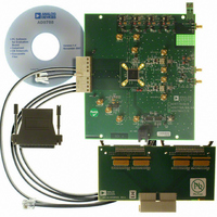
BOARD EVAL FOR AD9785
Manufacturer
Analog Devices Inc
Series
TxDAC®r
Datasheet
1.AD9785BSVZ.pdf
(64 pages)
Specifications of AD9785-EBZ
Number Of Dac's
2
Number Of Bits
12
Outputs And Type
2, Differential
Sampling Rate (per Second)
800M
Data Interface
Serial
Settling Time
22ms
Dac Type
Current
Voltage Supply Source
Analog and Digital
Operating Temperature
-40°C ~ 85°C
Utilized Ic / Part
AD9785
Silicon Manufacturer
Analog Devices
Application Sub Type
DAC
Kit Application Type
Data Converter
Silicon Core Number
AD9785
Kit Contents
Board
Lead Free Status / RoHS Status
Lead free / RoHS Compliant
Lead Free Status / RoHS Status
Lead free / RoHS Compliant, Lead free / RoHS Compliant


AD9785/AD9787/AD9788
There are two phases to a communication cycle with the
AD9785/AD9787/AD9788. Phase 1 is the instruction cycle,
which is the writing of an instruction byte into the AD9785/
AD9787/AD9788, coincident with the first eight SCLK rising
edges. The instruction byte provides the AD9785/AD9787/
AD9788 serial port controller with information regarding the
data transfer cycle, which is Phase 2 of the communication
cycle. The instruction byte defines whether the upcoming data
transfer is read or write and the serial address of the register
being accessed.
The first eight SCLK rising edges of each communication cycle
are used to write the instruction byte into the AD9785/AD9787/
AD9788. The remaining SCLK edges are for Phase 2 of the
communication cycle. Phase 2 is the actual data transfer
between the AD9785/AD9787/AD9788 and the system
controller. The number of bytes transferred during Phase 2 of
the communication cycle is a function of the register being
accessed.
For example, when accessing the frequency tuning word (FTW)
register, which is four bytes wide, Phase 2 requires that four
bytes be transferred. If accessing the amplitude scale factor (ASF)
register, which is three bytes wide, Phase 2 requires that three
bytes be transferred. After transferring all data bytes per the
instruction byte, the communication cycle is completed.
At the completion of any communication cycle, the AD9785/
AD9787/AD9788 serial port controller expects the next eight
rising SCLK edges to be the instruction byte of the next
communication cycle.
All data input is registered on the rising edge of SCLK. All data
is driven out of the AD9785/AD9787/AD9788 on the falling
edge of SCLK.
Rev. A | Page 22 of 64
Figure 43 through Figure 46 are useful in understanding the
general operation of the AD9785/AD9787/AD9788 serial port.
SPI_SDIO
SPI_SDIO
SPI_SDIO
SPI_SDIO
SPI_CSB
SPI_SDO
SPI_CSB
SPI_SDO
SPI_CSB
SPI_CSB
SPI_SDO
SCLK
SCLK
SCLK
SCLK
Figure 43. Serial Register Interface Timing, MSB First
Figure 46. SPI Register Read Timing Instruction Byte
Figure 44. Serial Register Interface Timing, LSB First
R/W N1 N0
A0
INSTRUCTION CYCLE
INSTRUCTION BIT 7
INSTRUCTION CYCLE
A1 A2
t
t
DS
DS
Figure 45. SPI Register Write Timing
DATA BIT n
A4 A3
A3 A4
t
PWH
t
t
DV
DH
t
A2 A1
N0 N1 R/W D0
SCLK
t
PWL
INSTRUCTION BIT 6
A0 D7 D6
DATA BIT n–1
D0
D7 D6
0
0
DATA TRANSFER CYCLE
DATA TRANSFER CYCLE
D1
D1
N
N
0
0
D5
D5
D2
D2
N
N
0
0
D3
D4
D4
D3
0
N
0
N
D2
D5
D5
D2
0
0
N
N
D6
D1
D1
D6
0
N
0
N
D0
D7
D7
D0
0
0
N
N
Related parts for AD9785-EBZ
Image
Part Number
Description
Manufacturer
Datasheet
Request
R

Part Number:
Description:
Dual 16B, 1.0 GSPS TxDAC
Manufacturer:
Analog Devices Inc
Datasheet:

Part Number:
Description:
±1.7g Dual-Axis IMEMS Accelerometer Evaluation Board
Manufacturer:
Analog Devices Inc
Datasheet:
Part Number:
Description:
Inertial Sensor Evaluation System
Manufacturer:
Analog Devices Inc
Datasheet:
Part Number:
Description:
Manufacturer:
Analog Devices Inc
Datasheet:
Part Number:
Description:
Manufacturer:
Analog Devices Inc
Datasheet:
Part Number:
Description:
Manufacturer:
Analog Devices Inc
Datasheet:
Part Number:
Description:
Manufacturer:
Analog Devices Inc
Datasheet:
Part Number:
Description:
Manufacturer:
Analog Devices Inc
Datasheet:
Part Number:
Description:
Manufacturer:
Analog Devices Inc
Datasheet:
Part Number:
Description:
Manufacturer:
Analog Devices Inc
Datasheet:
Part Number:
Description:
Manufacturer:
Analog Devices Inc
Datasheet:
Part Number:
Description:
Manufacturer:
Analog Devices Inc
Datasheet:
Part Number:
Description:
Manufacturer:
Analog Devices Inc
Datasheet: