AD9785-EBZ Analog Devices Inc, AD9785-EBZ Datasheet - Page 24
AD9785-EBZ
Manufacturer Part Number
AD9785-EBZ
Description
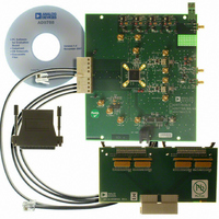
BOARD EVAL FOR AD9785
Manufacturer
Analog Devices Inc
Series
TxDAC®r
Datasheet
1.AD9785BSVZ.pdf
(64 pages)
Specifications of AD9785-EBZ
Number Of Dac's
2
Number Of Bits
12
Outputs And Type
2, Differential
Sampling Rate (per Second)
800M
Data Interface
Serial
Settling Time
22ms
Dac Type
Current
Voltage Supply Source
Analog and Digital
Operating Temperature
-40°C ~ 85°C
Utilized Ic / Part
AD9785
Silicon Manufacturer
Analog Devices
Application Sub Type
DAC
Kit Application Type
Data Converter
Silicon Core Number
AD9785
Kit Contents
Board
Lead Free Status / RoHS Status
Lead free / RoHS Compliant
Lead Free Status / RoHS Status
Lead free / RoHS Compliant, Lead free / RoHS Compliant


AD9785/AD9787/AD9788
SPI REGISTER MAP
When reading Table 9, note that the AD9785/AD9787/AD9788 is a 32-bit part and, therefore, the 4
with the MSB and ending with the LSB) represent a set of eight bits. Refer to the Bit Range column for the actual bits being described.
Table 9.
Address
0x00
0x01
0x02
0x03
0x04
0x05
0x06
0x07
0x08
0x09
0x0A
Register
Name
Comm.
(COMM)
Register
Digital
Control
Register
Data Sync
Control
Register
Multichip
Sync
Control
Register
PLL
Control
Register
I DAC
Control
Register
Auxiliary
DAC 1
Control
Register
Q DAC
Control
Register
Auxiliary
DAC 2
Control
Register
Interrupt
Control
Register
Frequency
Tuning
Word
Register
Bit
Range
[7:0]
[7:0]
[15:8]
[7:0]
[15:8]
[7:0]
[15:8]
[23:16]
[31:24]
[7:0]
[15:8]
[23:16]
[7:0]
[15:8]
[7:0]
[15:8]
[7:0]
[15:8]
[7:0]
[15:8]
[7:0]
[15:8]
[31:0]
Data Timing
Data timing
MSB
SPI_SDIO
bidirectional
(active high,
3-wire)
Reserved
Margin [0]
PLL enable
I DAC sleep
Auxiliary
DAC 1 sign
Q DAC sleep
Auxiliary
DAC 2 sign
error IRQ
Interpolation Factor [1:0]
VCO Control Voltage [2:0]
MSB − 1
LSB first
Clear phase
accumulator
LVDS data
clock enable
PLL VCO Divisor [1:0]
I DAC
power-down
Auxiliary
DAC 1
current
direction
Q DAC
power-down
Auxiliary
DAC 2
current
direction
Sync timing
error IRQ
Reserved
Clock State [3:0]
Correlate Threshold [4:0]
DATACLK Delay [4:0]
SYNC _O Delay [4:0]
SYNC_I Delay [4:0]
PLL Band Select [5:0]
Rev. A | Page 24 of 64
MSB − 2
Software
reset
Data
format
PN code
sync
enable
DATACLK
invert
Auxiliary
DAC 1
power-
down
Auxiliary
DAC 2
power-
down
Data
timing
error
type
Frequency Tuning Word [31:0]
Q DAC Gain Adjustment [7:0]
I DAC Gain Adjustment [7:0]
Auxiliary DAC 1 Data [7:0]
Auxiliary DAC 2 Data [7:0]
MSB − 3
Power-
down
mode
Single-
port
mode
Sync
mode
select
DATACLK
delay
enable
PLL Loop Divisor [1:0]
Sync
timing
error
type
Clear lock
indicator
(self-
reset)
Reserved
Reserved
MSB − 4
Auto
power-
down
enable
Real
mode
Pulse
sync
enable
Data
timing
mode
PLL lock
indicator
Sync
lock
lost
status
Reserved
Reserved
PLL Loop Bandwidth [4:0]
Sync lock
status
Sync Timing Margin [3:0]
Reserved
MSB − 5
I/O
transfer
(self-
reset)
IQ select
invert
Reserved
Set high
Set high
Sync
error
check
mode
SYNC _I
enable
PLL Bias [2:0]
th
through the 11
Data Timing Margin [3:1]
MSB − 6
Automatic
I/O
transfer
enable
Q first
Inverse
sinc
enable
Data sync
polarity
SYNC_O
polarity
Set low
SYNC _O
enable
PLL VCO Drive [1:0]
Data port
IRQ enable
Q DAC Gain Adjustment
I DAC Gain Adjustment
Auxiliary DAC 1 Data
Auxiliary DAC 2 Data
Reserved
th
[9:8]
[9:8]
[9:8]
[9:8]
columns (beginning
LSB
Open
Modulator
gain
control
DATACLK
output
enable
Reserved
Sync
loopback
enable
DATACLK
input
Set low
Sync port
IRQ
enable
Default
0x02
0x00
0x31
0x00
0x00
0x00
0x00
0x00
0x80
0xCF
0x37
0x38
0xF9
0x01
0x00
0x00
0xF9
0x01
0x00
0x00
0x00
0x00
0x00
Related parts for AD9785-EBZ
Image
Part Number
Description
Manufacturer
Datasheet
Request
R

Part Number:
Description:
Dual 16B, 1.0 GSPS TxDAC
Manufacturer:
Analog Devices Inc
Datasheet:

Part Number:
Description:
±1.7g Dual-Axis IMEMS Accelerometer Evaluation Board
Manufacturer:
Analog Devices Inc
Datasheet:
Part Number:
Description:
Inertial Sensor Evaluation System
Manufacturer:
Analog Devices Inc
Datasheet:
Part Number:
Description:
Manufacturer:
Analog Devices Inc
Datasheet:
Part Number:
Description:
Manufacturer:
Analog Devices Inc
Datasheet:
Part Number:
Description:
Manufacturer:
Analog Devices Inc
Datasheet:
Part Number:
Description:
Manufacturer:
Analog Devices Inc
Datasheet:
Part Number:
Description:
Manufacturer:
Analog Devices Inc
Datasheet:
Part Number:
Description:
Manufacturer:
Analog Devices Inc
Datasheet:
Part Number:
Description:
Manufacturer:
Analog Devices Inc
Datasheet:
Part Number:
Description:
Manufacturer:
Analog Devices Inc
Datasheet:
Part Number:
Description:
Manufacturer:
Analog Devices Inc
Datasheet:
Part Number:
Description:
Manufacturer:
Analog Devices Inc
Datasheet: