EVAL-AD5821EBZ Analog Devices Inc, EVAL-AD5821EBZ Datasheet - Page 4
EVAL-AD5821EBZ
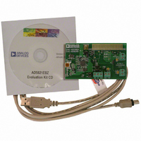
Manufacturer Part Number
EVAL-AD5821EBZ
Description
BOARD EVALUATION FOR AD5821
Manufacturer
Analog Devices Inc
Datasheet
1.AD5821ABCBZ-REEL7.pdf
(16 pages)
Specifications of EVAL-AD5821EBZ
Number Of Dac's
1
Number Of Bits
10
Outputs And Type
1, Single Ended
Sampling Rate (per Second)
400k
Data Interface
I²C
Settling Time
250µs
Dac Type
Current
Voltage Supply Source
Single
Operating Temperature
-30°C ~ 80°C
Utilized Ic / Part
AD5821
Lead Free Status / RoHS Status
Lead free / RoHS Compliant


AD5821
AC SPECIFICATIONS
V
Table 2.
Parameter
Output Current Settling Time
Slew Rate
Major Code Change Glitch Impulse
Digital Feedthrough
1
2
3
TIMING SPECIFICATIONS
V
Table 3.
Parameter
f
t
t
t
t
t
t
t
t
t
t
t
C
1
2
3
Timing Diagram
SCL
1
2
3
4
5
6
7
8
9
10
11
Temperature range is as follows: B Version = −40°C to +85°C.
Guaranteed by design and characterization; not production tested.
See the
Guaranteed by design and characterization; not production tested.
A master device must provide a hold time of at least 300 ns for the SDA signal (referred to the V
C
B
DD
DD
2
SDA
B
SCL
is the total capacitance of one bus line in pF. t
= 2.7 V to 5.5 V, AGND = DGND = 0 V, load resistance R
= 2.7 V to 3.6 V. All specifications T
Terminology
1
t
9
Limit at T
400
2.5
0.6
1.3
0.6
100
0.9
0
0.6
0.6
1.3
300
0
250
300
20 + 0.1 C
400
section.
3
CONDITION
START
B Version
t
4
MIN
B
3
, T
t
MAX
3
Min
B Version
MIN
R
and t
Typ
250
0.3
0.15
0.06
t
to T
Unit
kHz max
μs min
μs min
μs min
μs min
ns min
μs max
μs min
μs min
μs min
μs min
ns max
ns min
ns max
ns max
ns min
pF max
10
t
F
6
are measured between 0.3 V
MAX
1, 2
Figure 2. 2-Wire Serial Interface Timing Diagram
Max
, unless otherwise noted.
Unit
μs
nA-s
nA-s
mA/μs
Description
SCL clock frequency
SCL cycle time
t
t
t
t
t
t
t
t
t
May be CMOS driven
t
t
Capacitive load for each bus line
t
HIGH
LOW
HD, STA
SU, DAT
HD, DAT
SU, STA
SU, STO
BUF
R,
F
F
2
, fall time of SDA when receiving
, fall time of both SCL and SDA when transmitting
rise time of both SCL and SDA when receiving
Rev. 0 | Page 4 of 16
, bus free time between a stop condition and a start condition
, SCL low time
, SCL high time
L
, setup time for repeated start
, start/repeated start condition hold time
, data setup time
, stop condition setup time
= 25 Ω connected to V
, data hold time
Test Conditions/Comments
V
1 LSB change around major carry
t
11
DD
= 3.6 V, R
t
DD
5
and 0.7 V
INH MIN
L
of the SCL signal) to bridge the undefined region of the SCL falling edge.
= 25 Ω, L
DD
.
CONDITION
REPEATED
DD
L
START
, unless otherwise noted.
= 680 μH, ¼ scale to ¾ scale change (0x100 to 0x300)
t
7
t
4
t
1
CONDITION
STOP
t
8
Related parts for EVAL-AD5821EBZ
Image
Part Number
Description
Manufacturer
Datasheet
Request
R


Part Number:
Description:
BOARD EVAL FOR SI270X-A
Manufacturer:
Silicon Laboratories Inc
Datasheet:

Part Number:
Description:
BUCK CONV REF DESIGN KIT IP1201
Manufacturer:
International Rectifier
Datasheet:
Part Number:
Description:
BOARD DEMO SYNC DUAL BUCK CNVTER
Manufacturer:
International Rectifier
Datasheet:
Part Number:
Description:
BOARD DEMO SYNC BUCK CONVETER
Manufacturer:
International Rectifier
Datasheet:

Part Number:
Description:
EVALBOARD/EB Omnidirectional microphone - Analog
Manufacturer:
Analog Devices
Datasheet:
Part Number:
Description:
EVALBOARD/EB Omnidirectional microphone - Analog
Manufacturer:
Analog Devices
Datasheet:


Part Number:
Description:
BOARD EVAL LED DRIVER LT3756
Manufacturer:
Linear Technology
Datasheet:

Part Number:
Description:
BOARD EVAL FOR AD7741/7742
Manufacturer:
Analog Devices Inc
Datasheet:

Part Number:
Description:
±1.7g Dual-Axis IMEMS Accelerometer Evaluation Board
Manufacturer:
Analog Devices Inc
Datasheet:

Part Number:
Description:
IC MULTIPLIER ANALOG 8-SOIC T/R
Manufacturer:
Analog Devices Inc
Datasheet:

Part Number:
Description:
IC ANALOG MULTIPLIER 8-DIP
Manufacturer:
Analog Devices Inc
Datasheet:
Part Number:
Description:
IC ANALOG MULTIPLIER 8-SOIC
Manufacturer:
Analog Devices Inc
Datasheet:
Part Number:
Description:
IC ANALOG MULTIPLIER 8-DIP
Manufacturer:
Analog Devices Inc
Datasheet: