EVAL-AD5445EBZ Analog Devices Inc, EVAL-AD5445EBZ Datasheet - Page 18
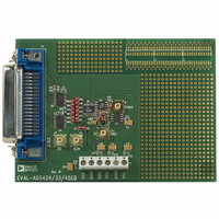
EVAL-AD5445EBZ
Manufacturer Part Number
EVAL-AD5445EBZ
Description
BOARD EVALUATION FOR AD5445
Manufacturer
Analog Devices Inc
Datasheet
1.AD5445YRUZ.pdf
(32 pages)
Specifications of EVAL-AD5445EBZ
Number Of Dac's
1
Number Of Bits
12
Outputs And Type
2, Single Ended
Sampling Rate (per Second)
20M
Data Interface
Parallel
Settling Time
30ns
Dac Type
Current
Voltage Supply Source
Single
Operating Temperature
-40°C ~ 125°C
Utilized Ic / Part
AD5445
Lead Free Status / RoHS Status
Lead free / RoHS Compliant


AD5424/AD5433/AD5445
BIPOLAR OPERATION
In some applications, it may be necessary to generate full
4-quadrant multiplying operation or a bipolar output swing.
This can be easily accomplished by using another external
amplifier and some external resistors, as shown in Figure 50. In
this circuit, the second amplifier, A2, provides a gain of 2.
Biasing the external amplifier with an offset from the reference
voltage, results in full 4-quadrant multiplying operation. The
transfer function of this circuit shows that both negative and
positive output voltages are created as the input data (D) is
incremented from code zero (V
0 V) to full scale (V
where D is the fractional representation of the digital word
loaded to the DAC and n is the resolution of the DAC.
When V
multiplication.
Table 8 shows the relationship between digital code and the
expected output voltage for bipolar operation (AD5424,
8-bit device).
Table 8. Bipolar Code Table
Digital Input
1111 1111
1000 0000
0000 0001
0000 0000
D = 0 to 255 (8-bit AD5424)
V
OUT
= 0 to 1023 (10-bit AD5433)
= 0 to 4095 (12-bit AD5445)
IN
is an ac signal, the circuit performs 4-quadrant
=
(
V
REF
×
OUT
D
2 /
V
±10V
= +V
REF
n
−1
)
REF
Analog Output (V)
+V
0
–V
–V
−
).
OUT
V
R1
REF
REF
REF
NOTES:
1.
2.
3.
REF
R1 AND R2 ARE USED ONLY IF GAIN ADJUSTMENT IS REQUIRED.
ADJUST R1 FOR V
MATCHING AND TRACKING IS ESSENTIAL FOR RESISTOR PAIRS R3 AND R4.
C1 PHASE COMPENSATION (1pF TO 2pF) MAY BE REQUIRED IF A1/A2 IS
A HIGH SPEED AMPLIFIER.
(127/128)
(128/128)
(127/128)
= –V
INPUTS
V
DATA
REF
REF
V
DD
AD5424/
AD5433/
AD5445
) to midscale (V
R/W
V
DD
Figure 50. Bipolar Operation (4-Quadrant Multiplication)
CS
OUT
= 0V WITH CODE 10000000 LOADED TO DAC.
GND
R
FB
20kΩ
I
I
OUT
OUT
R3
1
2
R2
OUT
C1
Rev. B | Page 18 of 32
AGND
=
A1
Stability
In the I-to-V configuration, the I
inverting node of the op amp must be connected as closely as
possible and proper PCB layout techniques must be employed.
Since every code change corresponds to a step function, gain
peaking may occur if the op amp has limited GBP and there is
excessive parasitic capacitance at the inverting node. This
parasitic capacitance introduces a pole into the open-loop
response, which can cause ringing or instability in closed-
loop applications.
An optional compensation capacitor, C1, can be added in
parallel with R
Figure 50. Too small a value of C1 can produce ringing at the
output, while too large a value can adversely affect the settling
time. C1 should be found empirically, but 1 pF to 2 pF is
generally adequate for compensation.
10kΩ
R4
A2
FB
20kΩ
R5
for stability, as shown in Figure 49 and
V
OUT
= –V
REF
TO +V
OUT
of the DAC and the
REF
Related parts for EVAL-AD5445EBZ
Image
Part Number
Description
Manufacturer
Datasheet
Request
R


Part Number:
Description:
BOARD EVAL FOR SI270X-A
Manufacturer:
Silicon Laboratories Inc
Datasheet:

Part Number:
Description:
BUCK CONV REF DESIGN KIT IP1201
Manufacturer:
International Rectifier
Datasheet:
Part Number:
Description:
BOARD DEMO SYNC DUAL BUCK CNVTER
Manufacturer:
International Rectifier
Datasheet:
Part Number:
Description:
BOARD DEMO SYNC BUCK CONVETER
Manufacturer:
International Rectifier
Datasheet:

Part Number:
Description:
EVALBOARD/EB Omnidirectional microphone - Analog
Manufacturer:
Analog Devices
Datasheet:
Part Number:
Description:
EVALBOARD/EB Omnidirectional microphone - Analog
Manufacturer:
Analog Devices
Datasheet:


Part Number:
Description:
BOARD EVAL LED DRIVER LT3756
Manufacturer:
Linear Technology
Datasheet:

Part Number:
Description:
BOARD EVAL FOR AD7741/7742
Manufacturer:
Analog Devices Inc
Datasheet:

Part Number:
Description:
±1.7g Dual-Axis IMEMS Accelerometer Evaluation Board
Manufacturer:
Analog Devices Inc
Datasheet:

Part Number:
Description:
IC MULTIPLIER ANALOG 8-SOIC T/R
Manufacturer:
Analog Devices Inc
Datasheet:

Part Number:
Description:
IC ANALOG MULTIPLIER 8-DIP
Manufacturer:
Analog Devices Inc
Datasheet:
Part Number:
Description:
IC ANALOG MULTIPLIER 8-SOIC
Manufacturer:
Analog Devices Inc
Datasheet:
Part Number:
Description:
IC ANALOG MULTIPLIER 8-DIP
Manufacturer:
Analog Devices Inc
Datasheet: