CDB4398 Cirrus Logic Inc, CDB4398 Datasheet - Page 29
CDB4398
Manufacturer Part Number
CDB4398
Description
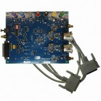
BOARD EVAL FOR CS4398 DAC
Manufacturer
Cirrus Logic Inc
Specifications of CDB4398
Number Of Dac's
2
Number Of Bits
24
Outputs And Type
2, Differential
Sampling Rate (per Second)
192k
Data Interface
I²C, SPI™
Dac Type
Voltage
Voltage Supply Source
Analog and Digital
Operating Temperature
-10°C ~ 70°C
Utilized Ic / Part
CS4398
Description/function
Audio D/A
Operating Supply Voltage
5 V
Product
Audio Modules
For Use With/related Products
CS4398
Lead Free Status / RoHS Status
Contains lead / RoHS non-compliant
Lead Free Status / RoHS Status
Lead free / RoHS Compliant, Contains lead / RoHS non-compliant
Other names
598-1155


DS568F1
7.
** All register access is R/W unless specified otherwise**
7.1
7.2
7.2.1
7.2.2
DSD_SRC
PART4
REGISTER DESCRIPTION
0
0
7
7
Chip ID - Register 01h
Function:
This register is Read-Only. Bits 7 through 3 are the part number ID, which is 01110b (14h), and the remain-
ing Bits (2 through 0) are for the chip revision (Rev. A = 000, Rev. B = 001, ...)
Mode Control 1 - Register 02h
Function:
When set to 0 (default), the dedicated DSD pins will be the active DSD inputs.
When set to 1, the source for DSD inputs will be as follows:
The dedicated DSD pins must be tied low while not in use.
Digital Interface Format (DIF2:0) BITs 6-4
Function:
These bits select the interface format for the serial audio input. The Functional Mode bits determine
whether PCM or DSD mode is selected.
PCM Mode: The required relationship between the Left/Right clock, serial clock and serial data is defined
by the Digital Interface Format, and the options are detailed in Figures 3 through 5.
DSD Input Source Select (DSD_SRC) BIT 7
DSDA input on SDATA pin
DSDB input on LRCK pin
DSD_SCLK input on SCLK pin
DIF2
0
0
0
0
1
1
1
1
PART3
DIF2
6
1
6
0
DIF1
0
0
1
1
0
0
1
1
PART2
DIF1
DIF0
5
1
5
0
0
1
0
1
0
1
0
1
Table 5. Digital Interface Formats - PCM Mode
Left-Justified, up to 24-bit data
I²S, up to 24-bit data
Right-Justified, 16-bit data
Right-Justified, 24-bit data
Right-Justified, 20-bit data
Right-Justified, 18-bit data
Reserved
Reserved
PART1
DIF0
1
0
4
4
Description
PART0
DEM1
3
0
3
0
DEM0
REV2
2
2
0
-
REV1
FM1
0
0
1
1
-
Format
(Default)
1
2
3
4
5
CS4398
REV0
FM0
Figure
0
0
0
-
3
4
5
5
5
5
29
Related parts for CDB4398
Image
Part Number
Description
Manufacturer
Datasheet
Request
R

Part Number:
Description:
Development Kit
Manufacturer:
Cirrus Logic Inc
Datasheet:
Part Number:
Description:
Development Kit
Manufacturer:
Cirrus Logic Inc
Datasheet:


Part Number:
Description:
High-efficiency PFC + Fluorescent Lamp Driver Reference Design
Manufacturer:
Cirrus Logic Inc
Datasheet:
Part Number:
Description:
Development Kit
Manufacturer:
Cirrus Logic Inc
Datasheet:
Part Number:
Description:
Development Kit
Manufacturer:
Cirrus Logic Inc
Datasheet:

Part Number:
Description:
Development Kit
Manufacturer:
Cirrus Logic Inc
Datasheet:
Part Number:
Description:
Development Kit
Manufacturer:
Cirrus Logic Inc
Datasheet:
Part Number:
Description:
Development Kit
Manufacturer:
Cirrus Logic Inc
Datasheet:
Part Number:
Description:
Development Kit
Manufacturer:
Cirrus Logic Inc
Datasheet:

Part Number:
Description:
EVALUATION BOARD FOR CS8427
Manufacturer:
Cirrus Logic Inc
Datasheet:

Part Number:
Description:
BOARD EVAL FOR CS8416 RCVR
Manufacturer:
Cirrus Logic Inc
Datasheet:

Part Number:
Description:
EVALUATION BOARD FOR CS8420
Manufacturer:
Cirrus Logic Inc
Datasheet:

Part Number:
Description:
KIT DEVELOPMENT EP9315 ARM9
Manufacturer:
Cirrus Logic Inc
Datasheet:

Part Number:
Description:
KIT DEVELOPMENT EP9302 ARM9
Manufacturer:
Cirrus Logic Inc
Datasheet: