MCP1631RD-DCPC1 Microchip Technology, MCP1631RD-DCPC1 Datasheet - Page 14
MCP1631RD-DCPC1
Manufacturer Part Number
MCP1631RD-DCPC1
Description
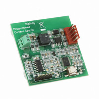
REF DES BATT CHARG OR LED DRIVER
Manufacturer
Microchip Technology
Datasheets
1.PIC16F616T-ISL.pdf
(214 pages)
2.MCP1631VHVT-330EST.pdf
(34 pages)
3.MCP1631VHVT-330EST.pdf
(32 pages)
Specifications of MCP1631RD-DCPC1
Current - Output / Channel
700mA
Outputs And Type
1, Non-Isolated
Features
Firmware for Li-Ion, NiMH, and NiCd Battery Charger
Voltage - Input
3.5 ~ 16 V
Utilized Ic / Part
MCP1631HV, PIC16F616
Core Chip
MCP1631HV, PIC16F616
Topology
Parallel, Series
Output Current
1A
No. Of Outputs
1
Input Voltage
3.5V To 16V
Dimming Control Type
Analog
Kit Contents
Board
Lead Free Status / RoHS Status
Lead free / RoHS Compliant
Voltage - Output
-
Lead Free Status / Rohs Status
Lead free / RoHS Compliant


PIC16F610/616/16HV610/616
2.2
The data memory (see Figure 2-4) is partitioned into
two banks, which contain the General Purpose
Registers (GPR) and the Special Function Registers
(SFR). The Special Function Registers are located in
the
PIC16F610/16HV610 Register locations 40h-7Fh in
Bank 0 are General Purpose Registers, implemented
as
locations 20h-7Fh in Bank 0 and A0h-BFh in Bank 1
are General Purpose Registers, implemented as static
RAM. Register locations F0h-FFh in Bank 1 point to
addresses 70h-7Fh in Bank 0. All other RAM is
unimplemented and returns ‘0’ when read. The RP0 bit
of the STATUS register is the bank select bit.
RP0
DS41288F-page 14
0
1
Note:
static
→
→
first
Data Memory Organization
Bank 0 is selected
Bank 1 is selected
The IRP and RP1 bits of the STATUS
register are reserved and should always be
maintained as ‘0’s.
RAM.
32
locations
PIC16F616/16HV616
of
each
Register
bank.
2.2.1
The register file is organized as 64 x 8 in the
PIC16F610/16HV610
PIC16F616/16HV616. Each register is accessed,
either directly or indirectly, through the File Select Reg-
ister (FSR) (see Section 2.4 “Indirect Addressing,
INDF and FSR Registers”).
2.2.2
The Special Function Registers are registers used by
the CPU and peripheral functions for controlling the
desired operation of the device (see Table 2-1). These
registers are static RAM.
The special registers can be classified into two sets:
core and peripheral. The Special Function Registers
associated with the “core” are described in this section.
Those related to the operation of the peripheral features
are described in the section of that peripheral feature.
GENERAL PURPOSE REGISTER
FILE
SPECIAL FUNCTION REGISTERS
© 2009 Microchip Technology Inc.
and
128 x 8
in
the
Related parts for MCP1631RD-DCPC1
Image
Part Number
Description
Manufacturer
Datasheet
Request
R

Part Number:
Description:
REFERENCE DESIGN MCP1631HV
Manufacturer:
Microchip Technology
Datasheet:

Part Number:
Description:
REFERENCE DESIGN FOR MCP1631HV
Manufacturer:
Microchip Technology
Datasheet:

Part Number:
Description:
Manufacturer:
Microchip Technology Inc.
Datasheet:
Part Number:
Description:
Manufacturer:
Microchip Technology Inc.
Datasheet:
Part Number:
Description:
Manufacturer:
Microchip Technology Inc.
Datasheet:
Part Number:
Description:
Manufacturer:
Microchip Technology Inc.
Datasheet:
Part Number:
Description:
Manufacturer:
Microchip Technology Inc.
Datasheet:
Part Number:
Description:
Manufacturer:
Microchip Technology Inc.
Datasheet:
Part Number:
Description:
Manufacturer:
Microchip Technology Inc.
Datasheet:
Part Number:
Description:
Manufacturer:
Microchip Technology Inc.
Datasheet: