MCP1631RD-DCPC1 Microchip Technology, MCP1631RD-DCPC1 Datasheet - Page 93
MCP1631RD-DCPC1
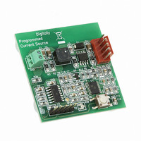
Manufacturer Part Number
MCP1631RD-DCPC1
Description
REF DES BATT CHARG OR LED DRIVER
Manufacturer
Microchip Technology
Datasheets
1.PIC16F616T-ISL.pdf
(214 pages)
2.MCP1631VHVT-330EST.pdf
(34 pages)
3.MCP1631VHVT-330EST.pdf
(32 pages)
Specifications of MCP1631RD-DCPC1
Current - Output / Channel
700mA
Outputs And Type
1, Non-Isolated
Features
Firmware for Li-Ion, NiMH, and NiCd Battery Charger
Voltage - Input
3.5 ~ 16 V
Utilized Ic / Part
MCP1631HV, PIC16F616
Core Chip
MCP1631HV, PIC16F616
Topology
Parallel, Series
Output Current
1A
No. Of Outputs
1
Input Voltage
3.5V To 16V
Dimming Control Type
Analog
Kit Contents
Board
Lead Free Status / RoHS Status
Lead free / RoHS Compliant
Voltage - Output
-
Lead Free Status / Rohs Status
Lead free / RoHS Compliant


10.4
The Enhanced PWM Mode can generate a PWM signal
on up to four different output pins with up to 10-bits of
resolution. It can do this through four different PWM
Output modes:
• Single PWM
• Half-Bridge PWM
• Full-Bridge PWM, Forward mode
• Full-Bridge PWM, Reverse mode
To select an Enhanced PWM mode, the P1M bits of the
CCP1CON register must be set appropriately.
FIGURE 10-5:
TABLE 10-6:
© 2009 Microchip Technology Inc.
ECCP Mode
Single
Half-Bridge
Full-Bridge, Forward
Full-Bridge, Reverse
Note 1: The TRIS register value for each PWM output must be configured appropriately.
CCPR1H (Slave)
Duty Cycle Registers
Note 1:
Comparator
2: Clearing the CCP1CON register will relinquish ECCP control of all PWM output pins.
3: Any pin not used by an Enhanced PWM mode is available for alternate pin functions
PWM (Enhanced Mode)
CCPR1L
PR2
TMR2
Comparator
The 8-bit timer TMR2 register is concatenated with the 2-bit internal Q clock, or 2 bits of the prescaler to create the 10-bit
time base.
EXAMPLE PIN ASSIGNMENTS FOR VARIOUS PWM ENHANCED MODES
(1)
EXAMPLE SIMPLIFIED BLOCK DIAGRAM OF THE ENHANCED PWM MODE
Clear Timer2,
toggle PWM pin and
latch duty cycle
CCP1<1:0>
P1M
00
10
01
11
R
S
P1M<1:0>
Q
PIC16F610/616/16HV610/616
CCP1/P1A
Yes
Yes
Yes
Yes
PWM1CON
Controller
Output
2
CCP1/P1A
P1B
P1C
P1D
The PWM outputs are multiplexed with I/O pins and are
designated P1A, P1B, P1C and P1D. The polarity of the
PWM pins is configurable and is selected by setting the
CCP1M bits in the CCP1CON register appropriately.
Table 10-6 shows the pin assignments for each
Enhanced PWM mode.
Figure 10-5 shows an example of a simplified block
diagram of the Enhanced PWM module.
4
CCP1M<3:0>
Note:
P1B
Yes
Yes
Yes
No
TRISC<5>
TRISC<4>
TRISC<3>
TRISC<2>
To
incomplete waveform when the PWM is
first enabled, the ECCP module waits until
the start of a new PWM period before
generating a PWM signal.
prevent
P1C
Yes
Yes
No
No
the
CCP1/P1A
P1B
P1C
P1D
generation
DS41288F-page 93
P1D
Yes
Yes
No
No
of
an
Related parts for MCP1631RD-DCPC1
Image
Part Number
Description
Manufacturer
Datasheet
Request
R

Part Number:
Description:
REFERENCE DESIGN MCP1631HV
Manufacturer:
Microchip Technology
Datasheet:

Part Number:
Description:
REFERENCE DESIGN FOR MCP1631HV
Manufacturer:
Microchip Technology
Datasheet:

Part Number:
Description:
Manufacturer:
Microchip Technology Inc.
Datasheet:
Part Number:
Description:
Manufacturer:
Microchip Technology Inc.
Datasheet:
Part Number:
Description:
Manufacturer:
Microchip Technology Inc.
Datasheet:
Part Number:
Description:
Manufacturer:
Microchip Technology Inc.
Datasheet:
Part Number:
Description:
Manufacturer:
Microchip Technology Inc.
Datasheet:
Part Number:
Description:
Manufacturer:
Microchip Technology Inc.
Datasheet:
Part Number:
Description:
Manufacturer:
Microchip Technology Inc.
Datasheet:
Part Number:
Description:
Manufacturer:
Microchip Technology Inc.
Datasheet: