RDK-194 Power Integrations, RDK-194 Datasheet - Page 2
RDK-194
Manufacturer Part Number
RDK-194
Description
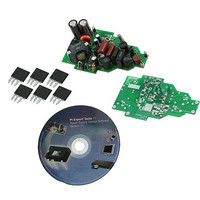
KIT REF DESIGN FOR LNK406EG
Manufacturer
Power Integrations
Type
Power Factor Correctionr
Specifications of RDK-194
Current - Output / Channel
500mA
Outputs And Type
1, Non-Isolated
Voltage - Output
28V
Features
Dimmable with Standard TRIAC Dimmer, Power Factor Correction
Voltage - Input
90 ~ 265VAC
Utilized Ic / Part
LNK406EG
Input Voltage
90 V to 265 V
Output Voltage
28 V
Product
Power Management Modules
Lead Free Status / RoHS Status
Lead free / RoHS Compliant
For Use With/related Products
LNK406EG
Other names
596-1308
Available stocks
Company
Part Number
Manufacturer
Quantity
Price
Company:

Part Number:
RDK-194
Manufacturer:
Power Integrations
Quantity:
135


Pin Functional Description
DRAIN (D) Pin:
This pin is the power MOSFET drain connection. It also
provides internal operating current for both start-up and
steady-state operation.
SOURCE (S) Pin:
This pin is the power MOSFET source connection. It is also the
ground reference for the BYPASS, FEEDBACK, REFERENCE and
VOLTAGE MONITOR pins.
BYPASS (BP) Pin:
This is the connection point for an external bypass capacitor for
the internally generated 5.9 V supply. This pin also provides
output power selection through choice of the BYPASS pin
capacitor value.
FEEDBACK (FB) Pin:
The FEEDBACK pin is used for output voltage feedback. The
current into the FEEDBACK pin is directly proportional to the
output voltage. The FEEDBACK pin also includes circuitry to
protect against open load and overload output conditions.
REFERENCE (R) Pin:
This pin is connected to an external precision resistor and is
used to configure for dimming (LNK403-409) and non-TRIAC
dimming (LNK413-419) modes of operation.
Rev. C 11/10
Figure 2.
LNK403-409EG/413-419EG
FEEDBACK (FB)
REFERENCE (R)
2
BYPASS (BP)
MONITOR (V)
VOLTAGE
Functional Block Diagram.
6.4 V
FEEDBACK
SENSE
SENSE
LINE
3-V
V
BG
1 V
T
UV/OV
I
CAPACITOR
LIM
BYPASS
SELECT
LOGIC
STOP
DC
FB
OFF
MAX
M
I
I
I
V
OSCILLATOR
FB
CLOCK
JITTER
REFERENCE
AUTO-RESTART
CONTROL
SOFT-START
PFC/CC
BLOCK
COUNTER
TIMER
+
-
Comparator
M
PRESENT
V
BG
I
VOLTAGE MONITOR (V) Pin:
This pin interfaces with an external input line peak detector,
consisting of a rectifier, filter capacitor and resistors. The
applied current is used to control stop logic for line under-
voltage (UV), overvoltage (OV), provide feed-forward to control
the output current and the remote ON/OFF function.
FAULT
Figure 3.
DC
FB
MAX
OFF
Exposed Pad
(backside) Internally
Connected to
SOURCE Pin (see
eSIP-7C Package
Drawing)
5.9 V
5.0 V
Pin Configuration.
UNDERVOLTAGE
BYPASS PIN
+
-
OCP
REGULATOR
HYSTERETIC
SHUTDOWN
THERMAL
E Package (eSIP-7C)
5.9 V
CURRENT LIMIT
COMPARATOR
(Top View)
Driver
Gate
PI-5431-102610
SenseFet
+
-
V
LEB
SENSE
www.powerint.com
I
LIM
I
S
7 D
5 S
4 BP
3 FB
2 V
1 R
PI-5432-060710
SOURCE (S)
DRAIN (D)
Related parts for RDK-194
Image
Part Number
Description
Manufacturer
Datasheet
Request
R

Part Number:
Description:
KIT REF DESIGN FOR LNK457D
Manufacturer:
Power Integrations
Datasheet:

Part Number:
Description:
REFERENCE DESIGN LINKSWITCH-PH
Manufacturer:
Power Integrations
Datasheet:

Part Number:
Description:
KIT REF DESIGN FOR LNK403EG
Manufacturer:
Power Integrations
Datasheet:

Part Number:
Description:
KIT REF DESIGN LINKSWITCH-CV
Manufacturer:
Power Integrations
Datasheet:

Part Number:
Description:
KIT REF DESIGN LINKSWITCH 2
Manufacturer:
Power Integrations
Datasheet:

Part Number:
Description:
Specifications: Family: Eval Boards - DC/DC & AC/DC (Off-Line) SMPS ; Series: HiperLCS™ ; Main Purpose: DC/DC, Step Down ; Outputs and Type: 1, Isolated ; Power - Output: 150W ; Voltage - Output: 24V ; Current - Output: 6.25A ; Voltage - Input:
Manufacturer:
Power Integrations, Inc.
Datasheet:

Part Number:
Description:
KIT DESIGN REF TINYSWITCH-III
Manufacturer:
Power Integrations
Datasheet:

Part Number:
Description:
KIT DESIGN REF LINKSWITCH LP
Manufacturer:
Power Integrations
Datasheet:

Part Number:
Description:
KIT REF DESIGN LED LINKSWITCH TN
Manufacturer:
Power Integrations
Datasheet:
Part Number:
Description:
KIT REF DESIGN PG LINKSWITCH-II
Manufacturer:
Power Integrations
Datasheet:
Part Number:
Description:
REFERENCE DESIGN LINKSWITCH-PL
Manufacturer:
Power Integrations
Datasheet:
Part Number:
Description:
REFERENCE DESIGN LINKSWITCH-PH
Manufacturer:
Power Integrations
Datasheet:

Part Number:
Description:
KIT REF DESIGN 36-72W MOTOR DRVR
Manufacturer:
Power Integrations
Datasheet:
Part Number:
Description:
Specifications: Manufacturer: Power Integrations ; Output Voltage: 380 VDC ; Input / Supply Voltage (Max): 264 VAC ; Input / Supply Voltage (Min): 90 VAC ; Mounting Style: Through Hole ; Output Current: 0.913 A ; Output Power: 347 W
Manufacturer:
Power Integrations, Inc.

Part Number:
Description:
KIT REF DESIGN TOP HX FOR TOP258
Manufacturer:
Power Integrations
Datasheet: