GENERAL DESCRIPTION
The AD8331 evaluation board is a platform for testing and
evaluating the AD8331 variable gain amplifier (VGA). The
board is provided completely assembled and tested; therefore,
the user only needs to connect an input signal, V
and a single 5 V power supply.
USER SUPPLIED OPTIONAL COMPONENTS
As shown in the schematic in Figure 2 (fixed), the board has
provisions for optional components. The basic components are
shown in black, and the optional components, which can be
installed at the user’s discretion, are shown in grey.
The input impedance of the LNA is configured for 50 Ω to
accommodate most signal generators and network analyzers.
Input impedances up to 6 kΩ can be realized by changing the
values of RFB and CSH. Consult the
details on this circuit feature. See Table 1 for typical values of
input impedance and corresponding components.
Table 1. LNA External Component Values for Common Source
Impedances
R
50
75
100
200
500
6 k
The board is designed for 0805 size surface-mount components.
Space is provided for various popular configurations of overload
diodes at locations D1, D2, or D3.
The LNA can be evaluated on its own. If so used alone, it must
be ac-coupled with capacitors at its differential output. Typical
values are 0.1 μF, and they are installed at Position C1 and
Position C2.
Resistors of 0 Ω are installed at R4 and R8, unless capacitive
loads larger than 10 pF are connected to the SMA connectors,
LON, and LOP (such as coaxial cables.) In that event, small
value resistors (68 Ω to 100 Ω) must be installed at R4 and R8.
A resistor can be inserted at RCLMP if output clamping is
desired. Consult the
Rev. A
Information furnished by Analog Devices is believed to be accurate and reliable. However, no
responsibility is assumed by Analog Devices for its use, nor for any infringements of patents or other
rights of third parties that may result from its use. Specifications subject to change without notice. No
license is granted by implication or otherwise under any patent or patent rights of Analog Devices.
Trademarks and registered trademarks are the property of their respective owners.
IN
(Ω)
RFB (Ω, Nearest 1% Value)
274
412
562
1.13 k
3.01 k
∞
AD8331
data sheet for appropriate values.
AD8331
data sheet for
GAIN
CSH (pF)
22
12
8
1.2
None
None
sources,
One Technology Way, P.O. Box 9106, Norwood, MA 02062-9106, U.S.A.
Tel: 781.329.4700
Fax: 781.461.3113
The preferred signal detection method is a differential probe
connected to VO, as shown in Figure 3. Single-ended loads can
be connected using the board edge SMA connector, VOH. Be
sure to take into account the 25.8 dB attenuation incurred when
using the board in this manner.
MEASUREMENT SETUP
The basic board connection for measuring bandwidth is shown
in Figure 3. A 5 V, 100 mA minimum power supply, and a low
noise, voltage reference supply for GAIN is required. Table 2
lists jumpers, and Figure 3 shows their function and positions.
Table 2. Jumper Functions
No.
ENBL
ENBV
W5, W6
Mode
HI_LO
BOARD LAYOUT AND PARTS LIST
The evaluation board circuitry uses four conductor layers. The
two inner layers are grounded, and all interconnecting circuitry
is located on the outer layers. Figure 5 to Figure 8 illustrate the
copper patterns. Table 3 is a part’s list.
Function
Enables the LNA when inserted in the top position
Enables the VGA when inserted in the top position
Connects the AD8331’s outputs to the SMA connectors
Bottom, gain increases with V
with V
Top, HI gain; bottom, LO gain (shown in Hi gain position)
AD8331 Evaluation Board
GAIN
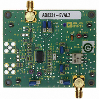
Figure 1. AD8331-EVAL Top View
©2006 Analog Devices, Inc. All rights reserved.
AD8331-EVAL
GAIN
; Top, gain decreases
www.analog.com