EVAL-ADXL345Z-DB Analog Devices Inc, EVAL-ADXL345Z-DB Datasheet - Page 15
EVAL-ADXL345Z-DB
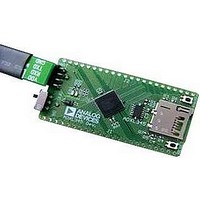
Manufacturer Part Number
EVAL-ADXL345Z-DB
Description
BOARD EVAL FOR ADXL345
Manufacturer
Analog Devices Inc
Series
iMEMS®r
Datasheets
1.EVAL-ADXL345Z.pdf
(40 pages)
2.EVAL-ADXL345Z.pdf
(2 pages)
3.EVAL-ADXL345Z.pdf
(12 pages)
Specifications of EVAL-ADXL345Z-DB
Sensor Type
Accelerometer, 3 Axis
Sensing Range
±2g, 4g, 8g, 16g
Interface
I²C, SPI
Sensitivity
256LSB/g, 128LSB/g, 64LSB/g, 32LSB/g
Voltage - Supply
2 V ~ 3.6 V
Embedded
No
Utilized Ic / Part
ADXL345
Silicon Manufacturer
Analog Devices
Application Sub Type
Accelerometer - Three-Axis
Kit Application Type
Sensing - Motion / Vibration / Shock
Silicon Core Number
ADXL345
Lead Free Status / RoHS Status
Lead free / RoHS Compliant


SERIAL COMMUNICATIONS
I
the ADXL345 operates as a slave. I
pin is tied high to V
to V
no default mode if the CS pin is left unconnected. Therefore, not
taking these precautions may result in an inability to communicate
with the part. In SPI mode, the CS pin is controlled by the bus
master. In both SPI and I
from the ADXL345 to the master device should be ignored
during writes to the ADXL345.
SPI
For SPI, either 3- or 4-wire configuration is possible, as shown in
the connection diagrams in Figure 34 and Figure 35. Clearing the
SPI bit (Bit D6) in the DATA_FORMAT register (Address 0x31)
selects 4-wire mode, whereas setting the SPI bit selects 3-wire
mode. The maximum SPI clock speed is 5 MHz with 100 pF
maximum loading, and the timing scheme follows clock polarity
(CPOL) = 1 and clock phase (CPHA) = 1. If power is applied to
the ADXL345 before the clock polarity and phase of the host
processor are configured, the CS pin should be brought high
before changing the clock polarity and phase. When using 3-wire
SPI, it is recommended that the SDO pin be either pulled up to
V
2
C and SPI digital communications are available. In both cases,
DD I/O
DD I/O
or pulled down to GND via a 10 kΩ resistor.
or be driven by an external controller because there is
Figure 34. 3-Wire SPI Connection Diagram
Figure 35. 4-Wire SPI Connection Diagram
ADXL345
ADXL345
DD I/O
SCLK
SCLK
SDIO
SDO
SDO
SDI
CS
CS
. The CS pin should always be tied high
2
C modes of operation, data transmitted
2
C mode is enabled if the CS
PROCESSOR
PROCESSOR
D OUT
D IN/OUT
D OUT
D OUT
D OUT
D IN
D OUT
Rev. B | Page 15 of 40
CS is the serial port enable line and is controlled by the SPI
master. This line must go low at the start of a transmission and
high at the end of a transmission, as shown in
is the serial port clock and is supplied by the SPI master. SCLK
should idle high during a period of no transmission. SDI and
SDO are the serial data input and output, respectively. Data is
updated on the falling edge of SCLK and should be sampled on
the rising edge of SCLK.
To read or write multiple bytes in a single transmission, the
multiple-byte bit, located after the R/ W bit in the first byte transfer
(MB in
addressing and the first byte of data, each subsequent set of
clock pulses (eight clock pulses) causes the ADXL345 to point
to the next register for a read or write. This shifting continues
until the clock pulses cease and
writes on different, nonsequential registers, CS must be deasserted
between transmissions and the new register must be addressed
separately.
The timing diagram for 3-wire SPI reads or writes is shown
in Figure 38. The 4-wire equivalents for SPI writes and reads
are shown in Figure 36 and Figure 37, respectively. For correct
operation of the part, the logic thresholds and timing parameters
in Table 9 and Table 10 must be met at all times.
Use of the 3200 Hz and 1600 Hz output data rates is only
recommended with SPI communication rates greater than or
equal to 2 MHz. The 800 Hz output data rate is recommended
only for communication speeds greater than or equal to 400 kHz,
and the remaining data rates scale proportionally. For example,
the minimum recommended communication speed for a 200 Hz
output data rate is 100 kHz. Operation at an output data rate
above the recommended maximum may result in undesirable
effects on the acceleration data, including missing samples or
additional noise.
Figure 36
to
Figure 38
CS is deasserted. To perform reads or
), must be set. After the register
Figure 36
ADXL345
. SCLK
Related parts for EVAL-ADXL345Z-DB
Image
Part Number
Description
Manufacturer
Datasheet
Request
R

Part Number:
Description:
IC, ADJ LDO REG, 1.5V TO 5V 250mA MSOP-8
Manufacturer:
Vishay
Datasheet:

Part Number:
Description:
IC, ADJ LDO REG, 1.5V TO 5V 0.6A 8-TSSOP
Manufacturer:
Vishay
Datasheet:
Part Number:
Description:
IC, ADJ LDO REG, 1.5V TO 5V 250mA MSOP-8
Manufacturer:
Vishay
Datasheet:

Part Number:
Description:
IC ADJ LDO REG 1.5V TO 5V 150mA 5-SOT-23
Manufacturer:
Vishay
Datasheet:

Part Number:
Description:
BOARD EVAL AS1324-AD
Manufacturer:
austriamicrosystems
Datasheet:
Part Number:
Description:
IC, ADJ LDO REG, 1.5V TO 5V 0.6A 8-TSSOP
Manufacturer:
Vishay
Datasheet:

Part Number:
Description:
IC, ADJ LDO REG, 1.5V TO 5V, 0.3A, MSOP8
Manufacturer:
Vishay
Datasheet:
Part Number:
Description:
IC, ADJ LDO REG, 1.5V TO 5V, 0.3A, MSOP8
Manufacturer:
Vishay
Datasheet:
Part Number:
Description:
IC, ADJ LDO REG 1.215V TO 5V 0.3A MSOP-8
Manufacturer:
Vishay
Datasheet:
Part Number:
Description:
IC, ADJ LDO REG 1.215V TO 5V 0.3A MSOP-8
Manufacturer:
Vishay
Datasheet:

Part Number:
Description:
±1.7g Dual-Axis IMEMS Accelerometer Evaluation Board
Manufacturer:
Analog Devices Inc
Datasheet:

Part Number:
Description:
IC MULTIPLIER ANALOG 8-SOIC T/R
Manufacturer:
Analog Devices Inc
Datasheet:

Part Number:
Description:
IC ANALOG MULTIPLIER 8-DIP
Manufacturer:
Analog Devices Inc
Datasheet:
Part Number:
Description:
IC ANALOG MULTIPLIER 8-SOIC
Manufacturer:
Analog Devices Inc
Datasheet:
Part Number:
Description:
IC ANALOG MULTIPLIER 8-DIP
Manufacturer:
Analog Devices Inc
Datasheet: