HW-V5-ML501-UNI-G Xilinx Inc, HW-V5-ML501-UNI-G Datasheet
HW-V5-ML501-UNI-G
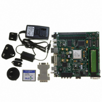
Specifications of HW-V5-ML501-UNI-G
Available stocks


Related parts for HW-V5-ML501-UNI-G


HW-V5-ML501-UNI-G Summary of contents
Page 1
ML501 Evaluation Platform User Guide UG226 (v1.4) August 24, 2009 R ...
Page 2
Xilinx is disclosing this user guide, manual, release note, and/or specification (the "Documentation") to you solely for use in the development of designs to operate with Xilinx hardware devices. You may not reproduce, distribute, republish, download, display, post, or transmit ...
Page 3
Table of Contents Preface: About This Guide Guide Contents . . . . . . . . . . . . . . . . . . . . . . . . . . . . . . . ...
Page 4
Xilinx XCF32P Platform Flash PROM Configuration Storage Device . . . . . . . . . . 30 24. JTAG Configuration Port . . . . . . . . . . . . . . . . ...
Page 5
R About This Guide The ML50x evaluation platforms enable designers to investigate and experiment with features of Virtex®-5 FPGAs. This user guide describes the features and operation of the ML501 Evaluation Platform. Guide Contents This manual contains the following chapters: ...
Page 6
Preface: About This Guide This guide describes the RocketIO™ GTP transceivers available in the Virtex-5 LXT and SXT platform devices. • Virtex-5 FPGA Tri-Mode Ethernet Media Access Controller User Guide This user guide describes the dedicated Tri-Mode Ethernet Media Access ...
Page 7
R Online Document The following conventions are used in this document: Convention Blue text Red text Blue, underlined text ML501 Evaluation Platform UG226 (v1.4) August 24, 2009 Typographical Conventions Meaning or Use Cross-reference link to a See the section location ...
Page 8
Preface: About This Guide 8 www.xilinx.com R ML501 Evaluation Platform UG226 (v1.4) August 24, 2009 ...
Page 9
R ML501 Evaluation Platform Introduction The ML501 Evaluation Platform enables designers to investigate and experiment with features of Virtex-5 LX FPGAs. This user guide describes features and operation of the ML501 Evaluation Platform. Features • Virtex-5 XC5VLX50-1FFG676 FPGA • 64-bit ...
Page 10
Chapter 1: ML501 Evaluation Platform • Xilinx XC95144XL CPLD for glue logic • Xilinx XCF32P Platform Flash PROM configuration storage device • JTAG configuration port for use with Parallel Cable III, Parallel Cable IV, or Platform USB download cable • ...
Page 11
R Block Diagram Figure 1-1 shows a block diagram of the ML501 Evaluation Platform (board). CPLD Misc. Glue Logic 16 Flash GPIO (Button/LED/DIP Switch) Piezo/Speaker PLL Clock Generator Plus User Oscillator System Monitor SMA (Differential In/Out Clocks) Dual PS/2 5V ...
Page 12
Chapter 1: ML501 Evaluation Platform Detailed Description The ML501 Evaluation Platform (board) is shown in page 13 (back). The numbered sections on the pages following the figures contain details on each feature ...
Page 13
R Note: The label on the CompactFlash (CF) card shipped with your board might differ from the one shown Figure 1-3: Detailed Description of Virtex-5 FPGA ML501 Evaluation Platform Components (Back) ML501 Evaluation Platform ...
Page 14
Chapter 1: ML501 Evaluation Platform 1. Virtex-5 FPGA A Xilinx Virtex-5 FPGA, XC5VLX50-1FFG676, is installed on the Evaluation Platform (the board). Configuration The board supports configuration in all modes: JTAG, Master Serial, Slave Serial, Master SelectMAP, Slave SelectMAP, Byte-wide Peripheral ...
Page 15
R Digitally Controlled Impedance Some FPGA banks can support the digitally controlled impedance (DCI) feature in Virtex-5 FPGAs. Support for DCI is summarized in Table 1-2: DCI Capability of FPGA Bank FPGA Bank ...
Page 16
Chapter 1: ML501 Evaluation Platform 2. DDR2 SODIMM The ML501 platform is shipped with a single-rank unregistered 256 MB SODIMM. The DDR2 SODIMM used is generally a Micron MT4HTF3264HY-53E or similar module. Serial Presence Detect (SPD) using an IIC interface ...
Page 17
R A differential clock output from the FPGA is driven out through a second pair of SMA connectors. This allows the FPGA to drive a precision clock to an external device such as a piece of test equipment. Table 1-3: ...
Page 18
Chapter 1: ML501 Evaluation Platform 4. Oscillator Sockets The board has one crystal oscillator socket (X1) wired for standard LVTTL-type oscillators. It connects to the FPGA clock pin as shown in 100-MHz oscillator and is powered by the 3.3V supply. ...
Page 19
R Table 1-5: DIP Switch Connections (SW4) (Continued) SW4 GPIO_DIP_SW6 GPIO_DIP_SW7 GPIO_DIP_SW8 7. User and Error LEDs (Active-High) There are a total of 15 active-High LEDs directly controllable by the FPGA: • Eight green LEDs are general purpose LEDs arranged ...
Page 20
Chapter 1: ML501 Evaluation Platform 8. User Pushbuttons (Active-High) Five active-High user pushbuttons are available for general purpose usage and are arranged in a North-East-South-West-Center orientation (only the center one is cited in Figure 1-2, page Table 1-7: User Pushbutton ...
Page 21
R Table 1-9: Expansion I/O Differential Connections (J4) J4 Differential Pin Pair Pos ML501 Evaluation Platform UG226 (v1.4) August 24, 2009 Schematic Net Name ...
Page 22
Chapter 1: ML501 Evaluation Platform Single-Ended Expansion I/O Connectors Header J6 contains 32 single-ended signal connections to the FPGA I/Os. This permits the signals on this connector to carry high-speed, single-ended data. All single-ended signals on connector J6 are matched ...
Page 23
R Table 1-10: Expansion I/O Single-Ended Connections (J6) (Continued) J6 Pin Other Expansion I/O Connectors In addition to the high-speed I/O paths, additional I/O signals and power connections are available to support expansion cards plugged ...
Page 24
Chapter 1: ML501 Evaluation Platform Table 1-11: Additional Expansion I/O Connections (J5) J5 Pin Label 1 ...
Page 25
R 11. Stereo AC97 Audio Codec The ML501 board has an AC97 audio codec (U16) to permit audio processing. The Analog Devices AD1981 Audio Codec supports stereo 16-bit audio with up to 48-kHz sampling. The sampling rate for record and ...
Page 26
Chapter 1: ML501 Evaluation Platform 14. IIC Bus with 8-Kb EEPROM An IIC EEPROM (STMicroelectronics M24C08) is provided on the board to store non- volatile data such as an Ethernet MAC address. The EEPROM is located under the removable LCD ...
Page 27
R 17. System ACE and CompactFlash Connector The Xilinx System ACE CompactFlash (CF) configuration controller allows a Type I CompactFlash card to program the FPGA through the JTAG port. Both hardware and software data can be downloaded through the JTAG ...
Page 28
Chapter 1: ML501 Evaluation Platform Note: System ACE configuration is enabled by way of a DIP switch. See and Mode DIP Switches.” The board also features a System ACE failsafe mode. In this mode, if the System ACE controller detects ...
Page 29
... Ground ENA_PAUSE = 0 CONFIG2 V 2.5V ANEG[ CONFIG3 V 2.5V ANEG[ 2. HWCFG_MODE[ CONFIG4 LED_DUPLEX (Set by J40) (Set by J40) CONFIG5 V 2.5V DIS_FC = 1 CC CONFIG6 LED_RX SEL_BDT = 0 22. USB Controller with Host and Peripheral Ports A Cypress CY7C67300 embedded USB host controller provides USB connectivity for the board ...
Page 30
Chapter 1: ML501 Evaluation Platform 23. Xilinx XCF32P Platform Flash PROM Configuration Storage Device Xilinx XCF32P Platform Flash PROM configuration storage device offers a convenient and easy-to-use configuration solution for the FPGA. The Platform Flash PROM holds up to two ...
Page 31
R 5V Brick 26. AC Adapter and Input Power Switch/Jack The ML501 board ships with a 15W (5V @ 3A) AC adapter. The power connector 5.5 mm barrel type plug (center positive). For applications requiring ...
Page 32
Chapter 1: ML501 Evaluation Platform 31. Configuration Address and Mode DIP Switches The 8-position DIP switch (SW15) sets the address and mode of configuration. It also enables fallback configuration of the Platform Flash PROM and enables System ACE configuration. Table ...
Page 33
R 33. SPI Flash The ML501 board has a 16-Mb SPI Flash (ST Microelectronics M25P16). The SPI Flash can be used for FPGA configuration or to hold user data. The SPI Flash can be in-system programmed using a Xilinx download ...
Page 34
Chapter 1: ML501 Evaluation Platform 37. System Monitor The ML501 supports both the dedicated and the auxiliary analog inputs to the Virtex-5 FPGA System Monitor block. The VP and VN pins shown in dedicated pins, whereas the VAUXP[x], VAUXN[x] represent ...
Page 35
R Table 1-16: System Monitor Connections (Continued) External Input VAUXP[1] VAUXN[2] VAUXP[2] VAUXN[3] VAUXP[3] VAUXN[4] VAUXP[4] VAUXN[5] VAUXP[5] VAUXN[6] VAUXP[6] VAUXN[7] VAUXP[7] VAUXN[8] VAUXP[8] VAUXN[9] VAUXP[9] VAUXN[10] VAUXP[10] VAUXN[11] VAUXP[11] VAUXN[12] VAUXP[12] VAUXN[13] VAUXP[13] VAUXN[14] VAUXP[14] VAUXN[15] VAUXP[15] ML501 Evaluation ...
Page 36
Chapter 1: ML501 Evaluation Platform Configuration Options The FPGA on the ML501 Evaluation Platform can be configured by five major devices: • Xilinx download cable (JTAG) • System ACE controller (JTAG) • Platform Flash PROM • Linear Flash memory • ...
Page 37
R Platform Flash PROM Configuration The Platform Flash PROM can also be used to program the FPGA. The Platform Flash PROM can hold up to two configuration images (up to four with compression), which are selectable by the two least ...
Page 38
Chapter 1: ML501 Evaluation Platform 38 www.xilinx.com R ML501 Evaluation Platform UG226 (v1.4) August 24, 2009 ...
Page 39
R Programming the IDT Clock Chip Overview ML50x evaluation boards feature an Integrated Device Technology (IDT) 3.3V EEPROM Programmable Clock Generator that is pre-programmed at the factory. In the event the chip programming is changed, the instructions in this appendix ...
Page 40
Appendix A: Programming the IDT Clock Chip Figure A-2: Programming the IDT5V9885 on the ML50x Using iMPACT 8. To finish programming the chip, cycle the power by turning off the board power switch. 9. After turning the board back on, ...
Page 41
R References Documents supporting Virtex-5 FPGAs: 1. DS100, Virtex-5 FPGA Family Overview. 2. DS202, Virtex-5 FPGA Data Sheet: DC and Switching Characteristics. 3. UG190, Virtex-5 FPGA User Guide. 4. UG194, Virtex-5 FPGA Tri-Mode Ethernet Media Access Controller User Guide. 5. ...
Page 42
Appendix B: References 42 www.xilinx.com R ML501 Evaluation Platform UG226 (v1.4) August 24, 2009 ...