EDOSK2674 Renesas Electronics America, EDOSK2674 Datasheet
EDOSK2674
Specifications of EDOSK2674


Related parts for EDOSK2674


EDOSK2674 Summary of contents
Page 1
... EDOSK2674 U M SER ANUAL F H8/2674R OR M ICROCOMPUTER ...
Page 2
Preface Cautions 1. This document may be, wholly or partially, subject to change without notice. 2. All rights reserved. No one is permitted to reproduce or duplicate, in any form, a part or this entire document without Hitachi Micro Systems ...
Page 3
... T C ....................................................................................................................................................... 3 ABLE OF ONTENTS 1. I ....................................................................................................................................................... 5 NTRODUCTION 1.1. EDOSK2674 GENERAL BOARD LAYOUT.......................................................................................................... 5 1.2. EDOSK2674 ACTUAL BOARD LAYOUT............................................................................................................. 6 2. EDOSK2674 B D .............................................................................................................................. 7 LOCK IAGRAM 2.1. POWER SUPPLY................................................................................................................................................. 7 2.2. OPERATING MODES .......................................................................................................................................... 7 2.3. H8/2674R MICROCOMPUTER............................................................................................................................ 8 2.4. BOOT FLASH MEMORY...................................................................................................................................... 8 2.5. MAIN FLASH MEMORY....................................................................................................................................... 9 2.6. RAM ..................................................................................................................................................................... 9 2.7. SDRAM................................................................................................................................................................. 9 2 ...
Page 4
FUNCTIONAL..................................................................................................................................................... 34 10 .................................................................................................................................... 38 DDITIONAL NFORMATION 4 ...
Page 5
... The EDOSK2674 card is provided with the following memory types and densities: 512KBytes (8-bit x 512) Boot Flash memory 4MBytes (16-bit x 2M) Main Flash memory 8MBytes (16-bit x 4bank x 1M) SDRAM memory A Real-time clock (RTC) is fitted to the EDOSK2674 to provide current date and time information to the MCU. 1.1. EDOSK2674 G B ENERAL The general board layout shows the position of all major parts of the board ...
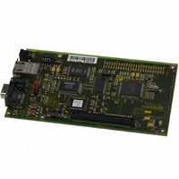
Page 6
... EDOSK2674 A B CTUAL OARD The actual board layout shows the real position of all components, the reference numbers and silk screen labelling. L AYOUT Figure 1-2: EDOSK Actual Board Layout 6 ...
Page 7
... EDOSK2674 B LOCK The EDOSK2674 is designed around a H8/2674R MCU and includes FLASH memory, SDRAM, real-time clock, an interface to a local expansion card, an interface for IO connections, a serial port and a LAN port. The figure below shows the block diagram of the EDOSK2674 board. Boot FLASH 512KByte ...
Page 8
... LASH EMORY The BOOT Flash memory is a 512K x 8bit PLCC device (AMD 29LV040B) and is fitted to a socket on the EDOSK2674. The MCU interfaces with the BOOT Flash on reset in area 0 only when the EDOSK is set to Boot mode. The same BOOT Flash is also accessible in area 7 when the EDOSK is set to either Boot or Normal mode. ...
Page 9
Extended CS period: T and T h 2.5. MAIN F M LASH EMORY The MAIN Flash memory is a 4MByte device (INTEL 28F320J3A) and is word accessed. The MCU interfaces with the MAIN Flash on reset in area 0 only ...
Page 10
EAL IME LOCK The EDOSK is supplied with a Real Time Clock (RTC) and battery backup (when fitted) for current date and time information. A cell retainer (J11) is used to hold a cell battery to ...
Page 11
E I XTERNAL NTERFACES Connector locations and pin orientation for Expansion and Auxiliary IO (right-angled 50-way IDC) is shown below: Pin 1 3. ERIAL NTERFACE The Serial Communication Interface (SCI-3) on the MCU directly supports three-wire serial ...
Page 12
LAN I NTERFACE A 10MHz LAN connection is provided through a standard RJ45 interface. Two LEDs are integrated into the Ethernet connector and give the following indication: Green: Link Indicator. Reflects the integrity status. Yellow: Activity Indicator. Activated by ...
Page 13
E C XPANSION ONNECTOR The EDOSK expansion bus connector is a 140-way JAE KX14-140K5D and has the following pin connections: Col: A Assignment Type I/O 1 GND - 2 CKIO O OUT 3 GND - I/O ...
Page 14
Col: A Assignment Type I/O 51 GND - 52 /WE0 O OUT 53 /WE2 O OUT 54 GND - 55 /WAIT0 I, P- /WAIT2 I, P- GND - 58 /IRQ1 I, P- /IRQ3 I, ...
Page 15
I/O Conn MCU Pin Symbol 43 44 P11 45 40 P73 47 36 P72 49 N/A No Connect T 3-4: A ABLE I/O Conn MCU Pin Symbol 44 45 P12 46 43 P10 48 N/A GND 50 N/A 3V3 I/O ...
Page 16
B O OARD PTIONS 4. UMPER INKS The EDOSK has a two-row 8 pin header for selecting operation modes. BOOT MON EN MF WEN BF WEN As default, jumpers for BOOT and MF WEN are fited. BOOT: ...
Page 17
Cell Battery D1 provides the Vcc supply and prevents the cell battery (or auxiliary supply) from powering all of the board when powered down. D2 provides protection for the cell battery (or auxiliary supply) against accidental charging. R (when fitted) ...
Page 18
The user may replace the HC49/U surface mounted AT cut crystal with another of similar type within the operating frequency of the MCU device. Please refer to the hardware manual for the MCU for the valid operating range. Another crystal ...
Page 19
TART UP NSTRUCTIONS 1. Connect the EDOSK notebook computer equipped with a nine pin D connector using a direct 1-1 cable (supplied). HOST PC F IGURE 2. Open a Hyper terminal set ...
Page 20
... ONITOR The H8/2674R has no dedicated debug port and at present SW has not been developed to enable a HDI monitor for the EDOSK2674. However, a MON_EN (monitor enable) jumper has been provided for this future feature. This jumper drives MCU port pin 30 Low when fitted and High when not fitted. HDI-Monitor code may be integrated with the user code and read the monitor enable jumper setting to enable or disable the feature ...
Page 21
... S OFTWARE The following map and register settings are for the H8/2674R fitted to the EDOSK2674 as standard i.e. with a system clock frequency of 33MHz. Registers are subject to change depending on the software requirements. 7.1. EDOSK2674 M M EMORY The addressable memory address space is split into eight areas, each capable of addressing 2Mbytes. Each area has a dedicated chip select signal (CS0n – ...
Page 22
Area 0 (CS0n) 1F FFFFh 20 0000h Area 1 (CS1n) 3F FFFFh 40 0000h Area 2 (CS2n) 5F FFFFh 60 0000h Area 3 (CS3n) 7F FFFFh 80 0000h Area 4 (CS4n) 9F FFFFh A0 0000h Area 5 (CS5n) ...
Page 23
H8/2674R R C EGISTER ONFIGURATION 7.2. ONTROLLER Bus Width Control Register: ABWCR (H’FFFEC0) = H’81 (BOOT) or H’80 (NORMAL) Bit Bit Name ABW7 ABW6 Initial Value 1/0 Note: In BOOT ...
Page 24
WTCRBH (H’FFFEC4) = H’71 Bit Bit Name Reserved W32 Initial Value 0 1 Area 3 has 7 program wait states inserted. SDRAM has a CAS Latency of 2. WTCRBL (H’FFFEC5) = H’23 (BOOT) or H’22 (NORMAL) Bit ...
Page 25
Burst ROM Interface Control Register: BROMCRH (H’FFFECA) = H’D3 (BOOT) or H’A3 (NORMAL) Bit Bit Name BSRMn BSTSn2 Initial Value Area 0 burst ROM enabled with maximum of 4 words. In BOOT mode ...
Page 26
SDRAM Notes: Prior to using the SDRAM the mode must be set in the SMR (SDRAM Mode Register). The SMR should be set to the value B’0000 0010 0000 – CAS latency 2, Burst 1. This is achieved by a ...
Page 27
... RTCOR6 Initial Value 1 1 Compare refresh count with 0xFF 7.2. NTERRUPT ONTROLLER The EDOSK2674 only uses the following interrupts: IRQ5n – Main Flash IRQ0n – LAN Controller IRQ1n-IRQ5n – Expansion connector NMI – Switch Interrupt Control Register: INTCR (H’FFFF31) = H’08 Bit No 7 ...
Page 28
S C ERIAL OMMUNICATION Serial Extension Mode Register: SEMR (H’FFFDA8) = H’00 Bit Bit Name Reserved Reserved Initial Value 0 0 Basic Clock is External; this register is not used. Serial Mode Register_2: SMR_2 (H’FFFF88) = ...
Page 29
W T ATCHDOG IMER Timer Control/Status Register: TCSR (H’FFFFBC) = H’18 Bit Bit Name OVF WT/IT Initial Value 0 0 Timer Counter: TCNT (H’FFFFBC-write / H’FFFFBD-read) = H’00 TCNT is an 8-bit readable/writable up-counter. TCNT is ...
Page 30
Port Function Control Register 1: PFCR1 (H’FFFE33) = H’FF Bit Bit Name A23E A22E Initial Value 1 1 Enable all Address lines (A21 and A23 used for SDRAM bank select) Port Function Control Register 2: PFCR2 (H’FFFE34) ...
Page 31
Enable SDRAM CS. Port 3 Register: PORT3 (H’FFFF52) Bit Bit Name Reserved Reserved Initial Value 0 0 Read only, value determined by the states of pins P35 to P30. Port 3 Open Drain Control Register: P3ODR (H’FFFE3C) ...
Page 32
Port H Data Direction Register: PHDDR (H’FFFF74) = H’0F Bit Bit Name Reserved Reserved Initial Value 0 0 The individual bits of PHDDR specify input or output for the pins of port H – ‘0’ input, ‘1’ ...
Page 33
M D ECHANICAL RAWING The mechanical drawing has been included here for the user to develop add-on boards and face plates. 33 ...
Page 34
... The JAE connector KX15-140K2D (shown) is fitted to the under-side of the Expansion Card to mate with KX14- 140K5D of the main board (in this case the EDOSK2674) with board to board space of 7mm. Components fitted to the under-side of the Expansion Card must have a maximum height of 2mm. ...
Page 35
... D0 to D15 may be used (Byte or Word access). D16 to D31 are not connected. Note: For an 8-bit mapped area D8 to D15 must be used. Read-Write Strobe The Expansion connector has a dedicated Read-Write signal (RWn). High indicates a read cycle and Low indicates a write cycle. EDOSK2674 Limitations- RWn signal is not connected. 35 ...
Page 36
... These are used to interrupt the main board processor. Depending upon the MCU IRQ may be level and/or edge triggered. To avoid contention the plug-in hardware should have the facility to select which of these used. EDOSK2674 Limitations- IRQ1n to IRQ4n may be used. IRQ5n may be used, but is also used by the Main Flash. ...
Page 37
... There are 2 DMA request and 2 DMA acknowledge, all active low, signals dedicated to the Expansion connector (DREQ0n, DREQ1n, DACK0n and DACK1n). These are used by the plug-in hardware to request and acknowledge a faster memory access. To avoid contention the plug-in hardware should have the facility to select which of these used. EDOSK2674 Limitations- All DMA signals may be used. 37 ...
Page 38
A I DDITIONAL NFORMATION For details on how to use Hitachi Embedded Workshop (HEW) refer to the HEW manual available on the CD or from the web site. For information about the H8 series microcomputers refer to the H8 ...