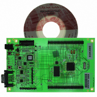
EDK3069 Renesas Electronics America, EDK3069 Datasheet
EDK3069
Specifications of EDK3069


Related parts for EDK3069


EDK3069 Summary of contents
Page 1
... EDK3069 U M SER ANUAL F 8/3069 FLASH M N CHIP ICROCONTROLLER ...
Page 2
Preface Cautions 1. This document may be, wholly or partially, subject to change without notice. 2. All rights reserved. No one is permitted to reproduce or duplicate, in any form, a part or this entire document without Hitachi Micro Systems ...
Page 3
T C ABLE OF ONTENTS ............................................................................................................................................. 3 ABLE OF ONTENTS ....................................................................................................................................... 4 TART UP NSTRUCTIONS 2.1. INSTALLING THE EVALUATION DEVELOPMENT KIT (EDK)........................................................................... 4 2.2. SERIAL CONNECTION ....................................................................................................................................... 4 2.3. POWER SUPPLY ................................................................................................................................................ ...
Page 4
TART UP NSTRUCTIONS 2. NSTALLING THE VALUATION Please refer to the quick start guide provided for initial installation of the EDK. A copy of the quick start guide and other information relating to this ...
Page 5
EDK B L OARD AYOUT The diagram shows a general layout of the EDK board. FLASH Programming Power NMI Switch BOOT LED Power LED User1 LED User2 LED RESET BOOT Switch Switch CJ5 9-Way D-Type CJ4 3.1. EDK B ...
Page 6
EDK O PERATION 4.1. USER INTERFACE The EDK provides three buttons for influencing the operation of the board. The purpose of each button is clearly marked next to it. Refer to the board layout for positions (Section 3) 1. ...
Page 7
... SRAM The SRAM device fitted to the board is a 4Mbit device allowing 256 x 16 operation. EDK3069 supports only 16-bit access. The H8/3069 microcontroller has chip select management built in. There is no external chip selection hardware associated with this device. The SRAM is connected to Chip Select 0 (CS0), which can address the range H’00080000 – H001FFFFF. ...
Page 8
M M EMORY AP Table 4-4 illustrates the EDK memory map for mode 5. H’000000 H’07FFFF H’080000 H’FEDFFF H’FEE000 H’FEE0FF H’FEE100 H’FFBF1F H’FFBF20 H’FFFF1F H’FFFF20 H’FFFFE9 H’FFFFEA H’FFFFFF 4.5. SRAM A T CCESS IMING External access timing is defined ...
Page 9
B O OARD PTIONS The EDK has a number of configuration settings set by jumpers CJ4 ( CJ5 ( and zero-ohm links. Common EDK functions can be set using the jumpers as described ...
Page 10
– CJ5 SER ODE ETTINGS CJ5 is used to set the operating mode of the microcontroller. These jumpers must be fitted at all times to ensure correct operation of the EDK. Jumper CJ 5-A User Mode ...
Page 11
ERIAL ORT ELECTION The programming serial port is connected to the RS232 connector by default. This allows direct programming of the EDK using the supplied software tools. A secondary serial port is available on the microcontroller ...
Page 12
... User MAT. Programming of the user boot mat can, however, only be performed in boot mode. For entry to User Boot mode on EDK3069, jumper D on jumper block CJ4 must be fitted 11-12, then the boot button depressed once. The Boot LED should light, suggesting a transition to user boot mode. ...
Page 13
S D TATE IAGRAM Async Boot Mode Controller : Positive Logic (CTS+BootSw) . /Res Waiting Reset Timer /Res ResSw . /Res Res /Res . Reset Reset (BootSW + ResSw + CTS) . /Res F 5-2: CPLD S D IGURE ...
Page 14
M H ICROCONTROLLER EADER The following table lists the connections to each or the headers on the board. 6. EADER Pin Function No 1 VSS PB7/RxD2/TP15 3 PB5/SCK2/LCASn/TP13 5 7 PB3/CS4n/DREQ1n/TMIO3/TP11 PB1/CS6n/DREQ0n/TMIO1/TP9 9 11 Vcl 13 PA6/TP6/TIOCA2/A21 ...
Page 15
C D ODE EVELOPMENT 7.1. HMON 7.1. ODE UPPORT The HMON library is built to support Modes and 7. The Device supports only these modes. 7.1. REAKPOINT UPPORT The monitor ...
Page 16
M M EMORY AP H'00000000 Vectors H'00001000 uGenU H'00001C78 H'00008000 CUser_Vectors H'00008003 H'00005000 PHMON CHMON H'00007A65 On-Chip FLASH ROM H'0007FFFF H'00080000 SRAM H'00083FFF H'00FEE000 Internal I/O REGISTERS H'00FEE0FF External Address Space H'00FFBF1F H'00FFBF20 On-Chip RAM H'00FFEC00 BHMON H'00FFEE0A H'00FFFD00 ...
Page 17
AUD ATE ETTING HMON has initially set to connect at 115200Baud. Should the user wish to change this, the value for the BRR in HMONserialconfiguser.c will need to be changed and the project re-built. Please refer ...