AD2S90-EB Analog Devices Inc, AD2S90-EB Datasheet - Page 11
AD2S90-EB
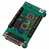
Manufacturer Part Number
AD2S90-EB
Description
BOARD EVAL FOR AD2S90
Manufacturer
Analog Devices Inc
Datasheet
1.AD2S90APZ.pdf
(12 pages)
Specifications of AD2S90-EB
Rohs Status
RoHS non-compliant


AD2S90/AD2S99 TYPICAL CONFIGURATION
Figure 21 shows a typical circuit configuration for the AD2S99
Oscillator and the AD2S90 Resolver-to-Digital Converter. The
maximum level of the SIN and COS input signals to the
AD2S90 should be 2 V rms 10%. All the analog ground sig-
nals should be star connected to the AD2S90 AGND pin. If
shielded twisted pair cables are used for the resolver signals, the
REV. D
REF
R2
R4
S2
RESOLVER
COS
S4
SIN
S3
S1
Figure 21. AD2S90 and AD2S99 Example Configuration
SEL2 = GND
SEL1 = V
F
OUT
= 5kHz
SS
NC = NO CONNECT
DGND
COS
–11–
SIN
NC
NC
4
5
6
7
8
shields should also be terminated at the AD2S90 AGND pin.
The SYNREF output of the AD2S99 should be connected to
the REF input pin of the AD2S90 via a 0.1 F capacitor with a
100 k resistor to GND. This is to block out any dc offset in
the SYNREF signal. For more detailed information please refer
to the AD2S99 data sheet.
0.1 F
19
20
1
2
3
3
9 10 11 12 13
(Not to Scale)
REF
COS LO
SIN LO
COS
AGND
SIN
18 17
AD2S99
TOP VIEW
4
2
50k
1
5
100k
(Not to Scale)
16 15
20 19
AD2S90
TOP VIEW
6
7
DGND
4.7 F
14
V
V
8
18
17
16
15
14
DD
SS
4.7 F
EXC
EXC
AGND
NC
NC
13
12
11
10
9
0.1 F
V
DD
4.7 F
4.7 F
0.1 F
V
SS
0.1 F
0.1 F
V
V
SS
DD
AD2S90
Related parts for AD2S90-EB
Image
Part Number
Description
Manufacturer
Datasheet
Request
R

Part Number:
Description:
±1.7g Dual-Axis IMEMS Accelerometer Evaluation Board
Manufacturer:
Analog Devices Inc
Datasheet:

Part Number:
Description:
Inertial Sensor Evaluation System
Manufacturer:
Analog Devices Inc
Datasheet:
Part Number:
Description:
Manufacturer:
Analog Devices Inc
Datasheet:
Part Number:
Description:
Manufacturer:
Analog Devices Inc
Datasheet:
Part Number:
Description:
Manufacturer:
Analog Devices Inc
Datasheet:
Part Number:
Description:
Manufacturer:
Analog Devices Inc
Datasheet:
Part Number:
Description:
Manufacturer:
Analog Devices Inc
Datasheet:
Part Number:
Description:
Manufacturer:
Analog Devices Inc
Datasheet:
Part Number:
Description:
Manufacturer:
Analog Devices Inc
Datasheet:
Part Number:
Description:
Manufacturer:
Analog Devices Inc
Datasheet:
Part Number:
Description:
Manufacturer:
Analog Devices Inc
Datasheet:
Part Number:
Description:
Manufacturer:
Analog Devices Inc
Datasheet:
Part Number:
Description:
Manufacturer:
Analog Devices Inc
Datasheet: