EVAL-AD5541/42EB Analog Devices Inc, EVAL-AD5541/42EB Datasheet - Page 14
EVAL-AD5541/42EB
Manufacturer Part Number
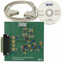
EVAL-AD5541/42EB
Description
BOARD EVAL FOR AD5541/42
Manufacturer
Analog Devices Inc
Datasheet
1.EVAL-AD554142EB.pdf
(20 pages)
Specifications of EVAL-AD5541/42EB
Number Of Dac's
1
Number Of Bits
16
Outputs And Type
1, Single Ended
Sampling Rate (per Second)
1.5M
Data Interface
Serial
Settling Time
1µs
Dac Type
Voltage
Voltage Supply Source
Single
Operating Temperature
-40°C ~ 85°C
Utilized Ic / Part
AD5541, AD5542
Lead Free Status / RoHS Status
Contains lead / RoHS non-compliant


AD5541/AD5542
MICROPROCESSOR INTERFACING
Microprocessor interfacing to the AD5541/AD5542 is via a
serial bus that uses standard protocol that is compatible with
DSP processors and microcontrollers. The communications
channel requires a 3- or 4-wire interface consisting of a clock
signal, a data signal and a synchronization signal. The
AD5541/AD5542 require a 16-bit data-word with data valid on
the rising edge of SCLK. The DAC update can be done
automatically when all the data is clocked in or it can be done
under control of the LDAC (AD5542 only).
AD5541/AD5542 TO ADSP-2101/ADSP-2103
INTERFACE
Figure 25 shows a serial interface between the AD5541/AD5542
and the ADSP-2101/ADSP-2103. The ADSP-2101/ADSP-2103
should be set to operate in the SPORT transmit alternate framing
mode. The ADSP-2101/ADSP-2103 are programmed through
the SPORT control register and should be configured as follows:
internal clock operation, active low framing, 16-bit word length.
Transmission is initiated by writing a word to the Tx register
after the SPORT has been enabled. As the data is clocked out
on each rising edge of the serial clock, an inverter is required
between the DSP and the DAC, because the AD5541/AD5542
clock data in on the falling edge of the SCLK.
AD5541/AD5542 TO 68HC11/68L11 INTERFACE
Figure 26 shows a serial interface between the AD5541/AD5542
and the 68HC11/68L11 microcontroller. SCK of the 68HC11/
68L11 drives the SCLK of the DAC, and the MOSI output drives
the serial data line serial DIN. The CS signal is driven from one
of the port lines. The 68HC11/68L11 is configured for master
mode: MSTR = 1, CPOL = 0, and CPHA = 0. Data appearing
on the MOSI output is valid on the rising edge of SCK.
Figure 25. AD5541/AD5542 to ADSP-2101/ADSP-2103 Interface
*ADDITIONAL PINS OMITTED FOR CLARITY.
**AD5542 ONLY.
*ADDITIONAL PINS OMITTED FOR CLARITY.
**AD5542 ONLY.
Figure 26. AD5541/AD5542 to 68HC11/68L11 Interface
ADSP-2103*
ADSP-2101/
68HC11/
68L11*
SCLK
MOSI
SCK
PC6
PC7
TFS
FO
DT
LDAC**
CS
DIN
SCLK
LDAC**
CS
DIN
SCLK
AD5542*
AD5542*
AD5541/
AD5541/
Rev. B | Page 14 of 20
AD5541/AD5542 TO MICROWIRE INTERFACE
Figure 27 shows an interface between the AD5541/AD5542
and any MICROWIRE-compatible device. Serial data is shifted
out on the falling edge of the serial clock and into the AD5541/
AD5542 on the rising edge of the serial clock. No glue logic is
required because the DAC clocks data into the input shift
register on the rising edge.
AD5541/AD5542 TO 80C51/80L51 INTERFACE
A serial interface between the AD5541/AD5542 and the 80C51/
80L51 microcontroller is shown in Figure 28. TxD of the micro-
controller drives the SCLK of the AD5541/AD5542, and RxD
drives the serial data line of the DAC. P3.3 is a bit programmable
pin on the serial port that is used to drive CS .
The 80C51/80L51 provide the LSB first, whereas the AD5541/
AD5542 expects the MSB of the 16-bit word first. Care should
be taken to ensure the transmit routine takes this into account.
When data is to be transmitted to the DAC, P3.3 is taken low.
Data on RxD is valid on the falling edge of TxD, so the clock
must be inverted as the DAC clocks data into the input shift
register on the rising edge of the serial clock. The 80C51/80L51
transmit data in 8-bit bytes with only eight falling clock edges
occurring in the transmit cycle. As the DAC requires a 16-bit
word, P3.3 must be left low after the first eight bits are transferred,
and brought high after the second byte is transferred. LDAC on
the AD5542 can also be controlled by the 80C51/ 80L51 serial
port output by using another bit programmable pin, P3.4.
*ADDITIONAL PINS OMITTED FOR CLARITY.
*ADDITIONAL PINS OMITTED FOR CLARITY.
**AD5542 ONLY.
MICROWIRE*
Figure 28. AD5541/AD5542 to 80C51/80L51 Interface
Figure 27. AD5541/AD5542 to MICROWIRE Interface
80C51/
80L51*
SCLK
P3.4
P3.3
RxD
TxD
CS
SO
LDAC**
CS
DIN
SCLK
CS
DIN
SCLK
AD5541/
AD5542*
AD5541/
AD5542*
Related parts for EVAL-AD5541/42EB
Image
Part Number
Description
Manufacturer
Datasheet
Request
R

Part Number:
Description:
IC, ADJ LDO REG, 1.5V TO 5V 250mA MSOP-8
Manufacturer:
Vishay
Datasheet:

Part Number:
Description:
IC, ADJ LDO REG, 1.5V TO 5V 0.6A 8-TSSOP
Manufacturer:
Vishay
Datasheet:
Part Number:
Description:
IC, ADJ LDO REG, 1.5V TO 5V 250mA MSOP-8
Manufacturer:
Vishay
Datasheet:

Part Number:
Description:
IC ADJ LDO REG 1.5V TO 5V 150mA 5-SOT-23
Manufacturer:
Vishay
Datasheet:

Part Number:
Description:
BOARD EVAL AS1324-AD
Manufacturer:
austriamicrosystems
Datasheet:
Part Number:
Description:
IC, ADJ LDO REG, 1.5V TO 5V 0.6A 8-TSSOP
Manufacturer:
Vishay
Datasheet:

Part Number:
Description:
IC, ADJ LDO REG, 1.5V TO 5V, 0.3A, MSOP8
Manufacturer:
Vishay
Datasheet:
Part Number:
Description:
IC, ADJ LDO REG, 1.5V TO 5V, 0.3A, MSOP8
Manufacturer:
Vishay
Datasheet:
Part Number:
Description:
IC, ADJ LDO REG 1.215V TO 5V 0.3A MSOP-8
Manufacturer:
Vishay
Datasheet:
Part Number:
Description:
IC, ADJ LDO REG 1.215V TO 5V 0.3A MSOP-8
Manufacturer:
Vishay
Datasheet:

Part Number:
Description:
±1.7g Dual-Axis IMEMS Accelerometer Evaluation Board
Manufacturer:
Analog Devices Inc
Datasheet:

Part Number:
Description:
IC MULTIPLIER ANALOG 8-SOIC T/R
Manufacturer:
Analog Devices Inc
Datasheet:

Part Number:
Description:
IC ANALOG MULTIPLIER 8-DIP
Manufacturer:
Analog Devices Inc
Datasheet:
Part Number:
Description:
IC ANALOG MULTIPLIER 8-SOIC
Manufacturer:
Analog Devices Inc
Datasheet:
Part Number:
Description:
IC ANALOG MULTIPLIER 8-DIP
Manufacturer:
Analog Devices Inc
Datasheet: