EVAL-AD7654CB Analog Devices Inc, EVAL-AD7654CB Datasheet - Page 8
EVAL-AD7654CB
Manufacturer Part Number
EVAL-AD7654CB
Description
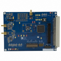
BOARD EVAL FOR AD7654
Manufacturer
Analog Devices Inc
Series
PulSAR®r
Specifications of EVAL-AD7654CB
Number Of Adc's
2
Number Of Bits
16
Sampling Rate (per Second)
500k
Data Interface
Serial, Parallel
Inputs Per Adc
2 Differential
Input Range
0 ~ 5 V
Power (typ) @ Conditions
120mW @ 500kSPS
Voltage Supply Source
Analog and Digital
Operating Temperature
-40°C ~ 85°C
Utilized Ic / Part
AD7654
Lead Free Status / RoHS Status
Contains lead / RoHS non-compliant


AD7654
PIN CONFIGURATION AND FUNCTION DESCRIPTIONS
Table 6. Pin Function Descriptions
Pin No.
1, 47, 48
2
3
4
5
6, 20
7
8
9, 10
11, 12
13
14
Mnemonic
AGND
AVDD
A0
BYTESWAP
A/B
DGND
IMPULSE
SER/PAR
D[0:1]
D[2:3] or
DIVSCLK[0:1]
D[4]
or EXT/INT
D[5]
or INVSYNC
Type
P
P
DI
DI
DI
P
DI
DI
DO
DI/O
DI/O
DI/O
1
Description
Analog Power Ground Pin.
Input Analog Power Pin. Nominally 5 V.
Multiplexer Select. When LOW, the analog inputs INA1 and INB1 are sampled simultaneously, then
converted. When HIGH, the analog inputs INA2 and INB2 are sampled simultaneously, then converted.
Parallel Mode Selection (8 bit, 16 bit). When LOW, the LSB is output on D[7:0] and the MSB is output on
D[15:8]. When HIGH, the LSB is output on D[15:8] and the MSB is output on D[7:0].
Data Channel Selection. In parallel mode, when LOW, the data from Channel B is read. When HIGH, the
data from Channel A is read. In serial mode, when HIGH, Channel A is output first followed by Channel
B. When LOW, Channel B is output first followed by Channel A.
Digital Power Ground.
Mode Selection. When HIGH, this input selects a reduced power mode. In this mode, the power
dissipation is approximately proportional to the sampling rate.
Serial/Parallel Selection Input. When LOW, the parallel port is selected; when HIGH, the serial interface
mode is selected and some bits of the DATA bus are used as a serial port.
Bit 0 and Bit 1 of the Parallel Port Data Output Bus. When SER/PAR is HIGH, these outputs are in high
impedance.
When SER/PAR is LOW, these outputs are used as Bit 2 and Bit 3 of the parallel port data output bus.
When SER/PAR is HIGH, EXT/INT is LOW, and RDC/SDIN is LOW, which is the serial master read after
convert mode, these inputs, part of the serial port, are used to slow down if desired the internal serial
clock that clocks the data output. In the other serial modes, these inputs are not used.
When SER/PARis LOW, this output is used as Bit 4 of the parallel port data output bus.
When SER/PARis HIGH, this input, part of the serial port, is used as a digital select input for choosing
the internal or an external data clock, called respectively, master and slave mode. With EXT/INT tied
LOW, the internal clock is selected on SCLK output. With EXT/INT set to a logic HIGH, output data is
synchronized to an external clock signal connected to the SCLK input.
When SER/PAR is LOW, this output is used as Bit 5 of the parallel port data output bus.
When SER/PAR is HIGH, this input, part of the serial port, is used to select the active state of the SYNC
signal in Master modes. When LOW, SYNC is active HIGH. When HIGH, SYNC is active LOW.
D2/DIVSCLK[0]
D3/DIVSCLK[1]
BYTESWAP
IMPULSE
SER/PAR
Figure 4. 48-Lead LQFP (ST-48) and 48-Lead LFCSP (CP-48)
AGND
DGND
AVDD
A/B
A0
D0
D1
10
11
12
1
2
3
4
5
6
7
8
9
48 47 46 45 44 43 42 41 40 39 38 37
13 14 15 16 17 18 19 20 21 22 23 24
PIN 1
Rev. B | Page 8 of 28
(Not to Scale)
AD7654
TOP VIEW
36
35
34
33
32
31
30
29
28
27
26
25
DVDD
CNVST
PD
RESET
CS
RD
EOC
BUSY
D15
D14
D13
D12
Related parts for EVAL-AD7654CB
Image
Part Number
Description
Manufacturer
Datasheet
Request
R

Part Number:
Description:
ENERCHIP CC EVAL KIT
Manufacturer:
Cymbet Corporation
Datasheet:

Part Number:
Description:
BOARD EVAL FOR AD976
Manufacturer:
Analog Devices Inc
Datasheet:

Part Number:
Description:
BOARD EVAL FOR ADXL345
Manufacturer:
Analog Devices Inc
Datasheet:

Part Number:
Description:
ENERCHIP CC SEH EVAL KIT
Manufacturer:
Cymbet Corporation
Datasheet:

Part Number:
Description:
ENERCHIP EP ENERGY HARVEST EVAL
Manufacturer:
Cymbet Corporation
Datasheet:

Part Number:
Description:
EVAL BOARD FOR TW6864-LB2-GR
Manufacturer:
Intersil
Datasheet:
Part Number:
Description:
EVAL BOARD FOR TW8816-LB3-GR
Manufacturer:
Intersil
Datasheet:
Part Number:
Description:
EVAL BOARD FOR TW8817-TA3-GRS
Manufacturer:
Intersil
Datasheet:

Part Number:
Description:
EVALUATION MODULE FOR ADUM4160
Manufacturer:
Analog Devices Inc
Datasheet:

Part Number:
Description:
BOARD EVALUATION ADCMP581BCP
Manufacturer:
Analog Devices Inc
Datasheet:
Part Number:
Description:
BOARD EVALUATION ADM1041
Manufacturer:
Analog Devices Inc
Datasheet:

Part Number:
Description:
EVAL BOARD FOR STM32F107VCT
Manufacturer:
STMicroelectronics
Datasheet:
Part Number:
Description:
BOARD EVAL FOR AD1954
Manufacturer:
Analog Devices Inc
Datasheet:
Part Number:
Description:
BOARD EVAL FOR AD1955
Manufacturer:
Analog Devices Inc
Datasheet:

Part Number:
Description:
BOARD EVAL FOR AD7655
Manufacturer:
Analog Devices Inc
Datasheet: