AD7476A-DBRD Analog Devices Inc, AD7476A-DBRD Datasheet - Page 20
AD7476A-DBRD
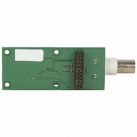
Manufacturer Part Number
AD7476A-DBRD
Description
BOARD EVAL FOR AD7476A
Manufacturer
Analog Devices Inc
Datasheet
1.AD7477AARMZ.pdf
(28 pages)
Specifications of AD7476A-DBRD
Design Resources
Output Channel Monitoring Using AD5380 (CN0008) AD5382 Channel Monitor Function (CN0012) AD5381 Channel Monitor Function (CN0013) AD5383 Channel Monitor Function (CN0015) AD5390/91/92 Channel Monitor Function (CN0030) Power off protected data acquisition signal chain using ADG4612 , AD711, and AD7476 (CN0165)
Number Of Adc's
*
Number Of Bits
*
Sampling Rate (per Second)
*
Data Interface
*
Inputs Per Adc
*
Input Range
*
Power (typ) @ Conditions
*
Voltage Supply Source
*
Operating Temperature
*
Utilized Ic / Part
AD7476A
Lead Free Status / RoHS Status
Contains lead / RoHS non-compliant


AD7476A/AD7477A/AD7478A
POWER VS. THROUGHPUT RATE
By using the power-down mode on the AD7476A/AD7477A/
AD7478A when not converting, the average power consump-
tion of the ADC decreases at lower throughput rates. Figure 23
shows that as the throughput rate is reduced, the device remains
in its power-down state longer and the average power consumption
over time drops accordingly.
For example, if the AD7476A/AD7477A/AD7478A operate in a
continuous sampling mode with a throughput rate of 100 kSPS
and an SCLK of 20 MHz (V
in the power-down mode between conversions, the power
consumption is calculated as follows:
The power dissipation during normal operation is 17.5 mW
(V
1 μs, and the remaining conversion time is another cycle, that is,
1 μs, then the AD7476A/AD7477A/AD7478A dissipate 17.5 mW
for 2 μs during each conversion cycle.
If the throughput rate is 100 kSPS, the cycle time is 10 μs, then
the average power dissipated during each cycle is (2/10) ×
(17.5 mW) = 3.5 mW.
DD
= 5 V). If the power-up time is one dummy cycle, that is,
DD
= 5 V) and the devices are placed
Rev. F | Page 20 of 28
If V
power-down mode between conversions, then the power
dissipation during normal operation is 5.1 mW. Thus, the
AD7576A/AD7477A/AD8478A dissipate 5.1 mW for 2 μs
during each conversion cycle. With a throughput rate of
100 kSPS, the average power dissipated during each cycle is
(2/10) × (5.1 mW) = 1.02 mW.
Figure 23 shows the power vs. the throughput rate when using
the power-down mode between conversions with both 5 V and
3 V supplies. The power-down mode is intended for use with
throughput rates of approximately 333 kSPS or less, because at
higher sampling rates, the power-down mode produces no
power savings.
DD
0.01
= 3 V, SCLK = 20 MHz, and the devices are again in
100
0.1
10
1
0
50
Figure 23. Power vs. Throughput
V
V
DD
DD
100
= 3V, SCLK = 20MHz
= 5V, SCLK = 20MHz
THROUGHPUT (kSPS)
150
200
250
300
350
Related parts for AD7476A-DBRD
Image
Part Number
Description
Manufacturer
Datasheet
Request
R

Part Number:
Description:
±1.7g Dual-Axis IMEMS Accelerometer Evaluation Board
Manufacturer:
Analog Devices Inc
Datasheet:

Part Number:
Description:
Inertial Sensor Evaluation System
Manufacturer:
Analog Devices Inc
Datasheet:
Part Number:
Description:
Manufacturer:
Analog Devices Inc
Datasheet:
Part Number:
Description:
Manufacturer:
Analog Devices Inc
Datasheet:
Part Number:
Description:
Manufacturer:
Analog Devices Inc
Datasheet:
Part Number:
Description:
Manufacturer:
Analog Devices Inc
Datasheet:
Part Number:
Description:
Manufacturer:
Analog Devices Inc
Datasheet:
Part Number:
Description:
Manufacturer:
Analog Devices Inc
Datasheet:
Part Number:
Description:
Manufacturer:
Analog Devices Inc
Datasheet:
Part Number:
Description:
Manufacturer:
Analog Devices Inc
Datasheet:
Part Number:
Description:
Manufacturer:
Analog Devices Inc
Datasheet:
Part Number:
Description:
Manufacturer:
Analog Devices Inc
Datasheet:
Part Number:
Description:
Manufacturer:
Analog Devices Inc
Datasheet: