AD7476A-DBRD Analog Devices Inc, AD7476A-DBRD Datasheet - Page 8
AD7476A-DBRD
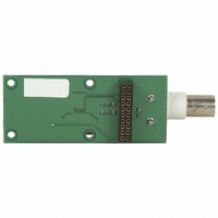
Manufacturer Part Number
AD7476A-DBRD
Description
BOARD EVAL FOR AD7476A
Manufacturer
Analog Devices Inc
Datasheet
1.AD7477AARMZ.pdf
(28 pages)
Specifications of AD7476A-DBRD
Design Resources
Output Channel Monitoring Using AD5380 (CN0008) AD5382 Channel Monitor Function (CN0012) AD5381 Channel Monitor Function (CN0013) AD5383 Channel Monitor Function (CN0015) AD5390/91/92 Channel Monitor Function (CN0030) Power off protected data acquisition signal chain using ADG4612 , AD711, and AD7476 (CN0165)
Number Of Adc's
*
Number Of Bits
*
Sampling Rate (per Second)
*
Data Interface
*
Inputs Per Adc
*
Input Range
*
Power (typ) @ Conditions
*
Voltage Supply Source
*
Operating Temperature
*
Utilized Ic / Part
AD7476A
Lead Free Status / RoHS Status
Contains lead / RoHS non-compliant


AD7476A/AD7477A/AD7478A
TIMING SPECIFICATIONS
V
Table 4.
Parameter
f
t
t
t
t
t
t
t
t
t
t
t
1
2
3
4
5
6
7
SCLK
CONVERT
QUIET
1
2
3
4
5
6
7
8
POWER-UP
Guaranteed by characterization. All input signals are specified with tr = tf = 5 ns (10% to 90% of V
Mark/space ratio for the SCLK input is 40/60 to 60/40.
Minimum f
Measured with the load circuit shown in Figure 2, and defined as the time required for the output to cross 0.8 V or 1.8 V when V
0.8 V or 2.0 V for V
Measured with a 50 pF load capacitor.
t
extrapolated back to remove the effects of charging or discharging the 50 pF capacitor. Therefore, the time, t
relinquish time of the part and is independent of the bus loading.
See the Power-Up Time section.
4
4
5
6
DD
8
is derived from the measured time taken by the data outputs to change 0.5 V when loaded with the circuit shown in Figure 2. The measured number is then
2
= 2.35 V to 5.25 V; T
7
SCLK
at which specifications are guaranteed.
Limit at T
10
20
20
16 × t
14 × t
12 × t
50
10
10
22
40
0.4 t
0.4 t
10
9.5
7
36
t
1
DD
7
values also apply to t
> 2.35 V.
SCLK
SCLK
SCLK
SCLK
SCLK
A
MIN
= T
, T
MAX
MIN
to T
MAX
8
minimum values
, unless otherwise noted.
Rev. F | Page 8 of 28
Unit
kHz min
kHz min
MHz max
ns min
ns min
ns min
ns max
ns max
ns min
ns min
ns min
ns min
ns min
ns max
ns min
μs max
1
3
3
Description
A, B grades
Y grade
AD7476A
AD7477A
AD7478A
Minimum quiet time required between bus relinquish
and start of next conversion
Minimum CS pulse width
CS to SCLK setup time
Delay from CS until SDATA three-state disabled
Data access time after SCLK falling edge
SCLK low pulse width
SCLK high pulse width
SCLK to data valid hold time
V
3.3 V < V
V
SCLK falling edge to SDATA high impedance
SCLK falling edge to SDATA high impedance
Power-up time from full power-down
DD
DD
DD
≤ 3.3 V
> 3.6 V
) and timed from a voltage level of 1.6 V.
DD
≤ 3.6 V
8
, quoted in the timing characteristics is the true bus
DD
= 2.35 V, and
Related parts for AD7476A-DBRD
Image
Part Number
Description
Manufacturer
Datasheet
Request
R

Part Number:
Description:
±1.7g Dual-Axis IMEMS Accelerometer Evaluation Board
Manufacturer:
Analog Devices Inc
Datasheet:

Part Number:
Description:
Inertial Sensor Evaluation System
Manufacturer:
Analog Devices Inc
Datasheet:
Part Number:
Description:
Manufacturer:
Analog Devices Inc
Datasheet:
Part Number:
Description:
Manufacturer:
Analog Devices Inc
Datasheet:
Part Number:
Description:
Manufacturer:
Analog Devices Inc
Datasheet:
Part Number:
Description:
Manufacturer:
Analog Devices Inc
Datasheet:
Part Number:
Description:
Manufacturer:
Analog Devices Inc
Datasheet:
Part Number:
Description:
Manufacturer:
Analog Devices Inc
Datasheet:
Part Number:
Description:
Manufacturer:
Analog Devices Inc
Datasheet:
Part Number:
Description:
Manufacturer:
Analog Devices Inc
Datasheet:
Part Number:
Description:
Manufacturer:
Analog Devices Inc
Datasheet:
Part Number:
Description:
Manufacturer:
Analog Devices Inc
Datasheet:
Part Number:
Description:
Manufacturer:
Analog Devices Inc
Datasheet: