TLP222G(F) Toshiba, TLP222G(F) Datasheet - Page 2
TLP222G(F)
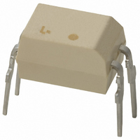
Manufacturer Part Number
TLP222G(F)
Description
IC PHOTOCOUPLER PHOTORELAY 4-DIP
Manufacturer
Toshiba
Series
TLP222Gr
Specifications of TLP222G(F)
Circuit
SPST-NO (1 Form A)
Output Type
AC, DC
On-state Resistance
50 Ohm
Load Current
120mA
Voltage - Input
1.15VDC
Voltage - Load
0 ~ 350 V
Mounting Type
Through Hole
Termination Style
PC Pin
Package / Case
4-DIP (0.300", 7.62mm)
Configuration
1 Channel
Isolation Voltage
2500 Vrms
Maximum Forward Diode Voltage
1.3 V
Minimum Forward Diode Voltage
1 V
Maximum Operating Temperature
+ 85 C
Minimum Operating Temperature
- 40 C
Forward Current
7.5 mA
Maximum Input Diode Current
25 mA
Maximum Reverse Diode Voltage
5 V
Output Device
Photo-MOSFET
Lead Free Status / RoHS Status
Lead free / RoHS Compliant
Other names
TLP222GF


Absolute Maximum Rating
Recommended Operating Conditions
Electrical Characteristics
Storage temperature range
Operating temperature range
Lead soldering temperature (10 s)
Isolation voltage (AC, 1 min, R.H. < = 60%)
Note: Using continuously under heavy loads (e.g. the application of high temperature/current/voltage and the
Note 1: Two channels operating simultaneously.
Note 2: Device considered a two-terminal device: LED side pins shorted together and detector side pins shorted
Supply voltage
Forward current
On-state current
Operating temperature
Note: Recommended operating conditions are given as a design guideline to obtain expected performance of the
Detector
Detector
LED
LED
significant change in temperature, etc.) may cause this product to decrease in the reliability significantly even
if the operating conditions (i.e. operating temperature/current/voltage, etc.) are within the absolute maximum
ratings.
Please design the appropriate reliability upon reviewing the Toshiba Semiconductor Reliability Handbook
(“Handling Precautions”/“Derating Concept and Methods”) and individual reliability data (i.e. reliability test
report and estimated failure rate, etc).
device. Additionally, each item is an independent guideline respectively. In developing designs using this
product, please confirm specified characteristics shown in this document.
Forward current
Forward current derating (Ta > = 25°C)
Peak forward current
(100 μs pulse, 100 pps)
Reverse voltage
Junction temperature
Off-state output terminal voltage
On-state
current
On-state
current
derating
(Ta > = 25°C)
Junction temperature
Forward voltage
Reverse current
Capacitance
Off-state current
Capacitance
together.
Characteristics
Characteristics
Characteristics
TLP222G
TLP222G-2 Two channel
TLP222G
TLP222G-2 Two channel
One channel
operation
operations
One channel
operation
operations
(Ta = 25°C)
(Ta = 25°C)
(Note 2)
(Note 1)
(Note 1)
Symbol
Symbol
C
V
I
T
I
OFF
V
C
ON
I
OFF
I
opr
DD
R
F
F
T
ΔI
Symbol
ΔI
V
I
V
V = 0, f = 1 MHz
V
V = 0, f = 1 MHz
BV
ON
T
T
T
F
I
I
V
F
OFF
ON
R
OFF
I
FP
T
T
Min
−20
opr
stg
sol
F
= 10 mA
⎯
⎯
/°C
R
5
j
j
2
/°C
S
= 5 V
= 350 V
Typ.
Test Condition
7.5
⎯
⎯
⎯
−55 to 125
−40 to 85
Rating
2500
−0.5
−1.2
125
350
120
125
260
Max
280
100
50
25
65
1
5
Unit
mA
mA
°C
V
mA/°C
mA/°C
Vrms
Unit
mA
mA
°C
°C
°C
°C
°C
TLP222G,TLP222G-2
A
V
V
Min
1.0
⎯
⎯
⎯
⎯
Typ.
1.15
30
30
⎯
⎯
2007-10-01
Max
1.3
10
⎯
⎯
1
Unit
μA
pF
μA
pF
V
Related parts for TLP222G(F)
Image
Part Number
Description
Manufacturer
Datasheet
Request
R

Part Number:
Description:
IC PHOTOCOUPLER PHOTORELAY 4-DIP
Manufacturer:
Toshiba
Datasheet:

Part Number:
Description:
PHOTOCOUPLER PHOTORELAY 8-DIP
Manufacturer:
Toshiba
Datasheet:

Part Number:
Description:
Cordless Telephones PBX Modems
Manufacturer:
Toshiba Semiconductor
Datasheet:

Part Number:
Description:
Toshiba Semiconductor [TOSHIBA IGBT Module Silicon N Channel IGBT]
Manufacturer:
TOSHIBA Semiconductor CORPORATION
Datasheet:
Part Number:
Description:
TOSHIBA GTR MODULE SILICON NPN TRIPLE DIFFUSED TYPE
Manufacturer:
TOSHIBA Semiconductor CORPORATION
Datasheet:
Part Number:
Description:
TOSHIBA GTR Module Silicon N Channel IGBT
Manufacturer:
TOSHIBA Semiconductor CORPORATION
Datasheet:
Part Number:
Description:
TOSHIBA Intelligent Power Module Silicon N Channel IGBT
Manufacturer:
TOSHIBA Semiconductor CORPORATION
Datasheet:
Part Number:
Description:
TOSHIBA INTELLIGENT POWER MODULE SILICON N CHANNEL LGBT
Manufacturer:
TOSHIBA Semiconductor CORPORATION
Datasheet:
Part Number:
Description:
TOSHIBA IGBT Module Silicon N Channel IGBT
Manufacturer:
TOSHIBA Semiconductor CORPORATION
Datasheet:
Part Number:
Description:
TOSHIBA GTR MODULE SILICON N−CHANNEL IGBT
Manufacturer:
TOSHIBA Semiconductor CORPORATION
Datasheet:
Part Number:
Description:
TOSHIBA Intelligent Power Module Silicon N Channel IGBT
Manufacturer:
TOSHIBA Semiconductor CORPORATION
Datasheet:
Part Number:
Description:
TOSHIBA GTR Module Silicon N Channel IGBT
Manufacturer:
TOSHIBA Semiconductor CORPORATION
Datasheet:
Part Number:
Description:
TOSHIBA INTELLIGENT POWER MODULE
Manufacturer:
TOSHIBA Semiconductor CORPORATION
Datasheet:
Part Number:
Description:
TOSHIBA Intelligent Power Module Silicon N Channel IGBT
Manufacturer:
TOSHIBA Semiconductor CORPORATION
Datasheet:
Part Number:
Description:
TOSHIBA Intelligent Power Module Silicon N Channel IGBT
Manufacturer:
TOSHIBA Semiconductor CORPORATION
Datasheet: