TLP222G(F) Toshiba, TLP222G(F) Datasheet - Page 74
TLP222G(F)
Manufacturer Part Number
TLP222G(F)
Description
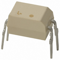
IC PHOTOCOUPLER PHOTORELAY 4-DIP
Manufacturer
Toshiba
Series
TLP222Gr
Specifications of TLP222G(F)
Circuit
SPST-NO (1 Form A)
Output Type
AC, DC
On-state Resistance
50 Ohm
Load Current
120mA
Voltage - Input
1.15VDC
Voltage - Load
0 ~ 350 V
Mounting Type
Through Hole
Termination Style
PC Pin
Package / Case
4-DIP (0.300", 7.62mm)
Configuration
1 Channel
Isolation Voltage
2500 Vrms
Maximum Forward Diode Voltage
1.3 V
Minimum Forward Diode Voltage
1 V
Maximum Operating Temperature
+ 85 C
Minimum Operating Temperature
- 40 C
Forward Current
7.5 mA
Maximum Input Diode Current
25 mA
Maximum Reverse Diode Voltage
5 V
Output Device
Photo-MOSFET
Lead Free Status / RoHS Status
Lead free / RoHS Compliant
Other names
TLP222GF


11
6
Zero-Crossing Phototriac Output: TLP561G/TLP561J and Mini-Flat TLP161G/TLP166J
Non-Zero Crossing Phototriac Output: TLP560G/TLP560J and Mini-Flat TLP160G/TLP260J
V
SSR and Power Control Circuit Applications
V
CC
CC
Photocoupler Application Circuit Examples
R
R
F
F
TLP160G / TLP560G / TLP3022 ( S )
TLP260J / TLP560J / TLP3052 ( S )
TLP161G/ TLP561G/ TLP3042 ( S )
TLP166J / TLP561J / TLP3062 ( S ) / TLP3082 ( S ) / TLP3782 ( S )
Waveforms
Waveforms
Lamp Load (1-A tungsten lamp)
Lamp Load (1-A tungsten lamp)
Top:
Medium:
Bottom:
Top:
Medium: V
Bottom:
ZC
I
V
I
I
I
F
T
F
T
T
T
20 mA/div
100 V/div
5 A/div
20 mA/div
100 V/div
5 A/div
G : 100 Ω
J : 200 Ω
R
R
T
R
G
G
74
Recommended
Recommended
conditions
conditions
L load (2.5-A pure inductive load)
L load (2.5-A pure inductive load)
R
C
R
C
S
S
S
S
TNR
TNR
I
R
R
I
R
R
R
F
F
G
S
T
G
S
= 20 mA
= 47 Ω
= 47 Ω, C
= 20 mA
= 100 Ω/200 Ω
= 47 Ω
= 47 Ω, C
AC Load
AC Load
S
S
= 0.033 μF
= 0.033 μF
G: 120 Vac
J: 240 Vac
G: 120 Vac
J: 240 Vac
Related parts for TLP222G(F)
Image
Part Number
Description
Manufacturer
Datasheet
Request
R

Part Number:
Description:
IC PHOTOCOUPLER PHOTORELAY 4-DIP
Manufacturer:
Toshiba
Datasheet:

Part Number:
Description:
PHOTOCOUPLER PHOTORELAY 8-DIP
Manufacturer:
Toshiba
Datasheet:

Part Number:
Description:
Cordless Telephones PBX Modems
Manufacturer:
Toshiba Semiconductor
Datasheet:

Part Number:
Description:
Toshiba Semiconductor [TOSHIBA IGBT Module Silicon N Channel IGBT]
Manufacturer:
TOSHIBA Semiconductor CORPORATION
Datasheet:
Part Number:
Description:
TOSHIBA GTR MODULE SILICON NPN TRIPLE DIFFUSED TYPE
Manufacturer:
TOSHIBA Semiconductor CORPORATION
Datasheet:
Part Number:
Description:
TOSHIBA GTR Module Silicon N Channel IGBT
Manufacturer:
TOSHIBA Semiconductor CORPORATION
Datasheet:
Part Number:
Description:
TOSHIBA Intelligent Power Module Silicon N Channel IGBT
Manufacturer:
TOSHIBA Semiconductor CORPORATION
Datasheet:
Part Number:
Description:
TOSHIBA INTELLIGENT POWER MODULE SILICON N CHANNEL LGBT
Manufacturer:
TOSHIBA Semiconductor CORPORATION
Datasheet:
Part Number:
Description:
TOSHIBA IGBT Module Silicon N Channel IGBT
Manufacturer:
TOSHIBA Semiconductor CORPORATION
Datasheet:
Part Number:
Description:
TOSHIBA GTR MODULE SILICON N−CHANNEL IGBT
Manufacturer:
TOSHIBA Semiconductor CORPORATION
Datasheet:
Part Number:
Description:
TOSHIBA Intelligent Power Module Silicon N Channel IGBT
Manufacturer:
TOSHIBA Semiconductor CORPORATION
Datasheet:
Part Number:
Description:
TOSHIBA GTR Module Silicon N Channel IGBT
Manufacturer:
TOSHIBA Semiconductor CORPORATION
Datasheet:
Part Number:
Description:
TOSHIBA INTELLIGENT POWER MODULE
Manufacturer:
TOSHIBA Semiconductor CORPORATION
Datasheet:
Part Number:
Description:
TOSHIBA Intelligent Power Module Silicon N Channel IGBT
Manufacturer:
TOSHIBA Semiconductor CORPORATION
Datasheet:
Part Number:
Description:
TOSHIBA Intelligent Power Module Silicon N Channel IGBT
Manufacturer:
TOSHIBA Semiconductor CORPORATION
Datasheet: