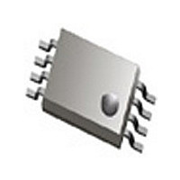
MC10EP01DT ON Semiconductor, MC10EP01DT Datasheet

MC10EP01DT
Specifications of MC10EP01DT
Available stocks
Related parts for MC10EP01DT
MC10EP01DT Summary of contents
Page 1
MC10EP01, MC100EP01 3.3V / 5V ECL 4-Input OR/NOR Description The MC10EP01 is a 4−input OR/NOR gate. The device is functionally equivalent to the EL01 device, LVEL01, and E101 (a quad version). With AC performance much faster than the LVEL01 device, the ...
Page 2
Figure 1. 8−Lead Pinout (Top View) and Logic Diagram Table 3. ATTRIBUTES Characteristics Internal Input Pulldown Resistor Internal Input Pullup Resistor ESD Protection Moisture Sensitivity, Indefinite Time Out of Drypack (Note 1) ...
Page 3
Table 4. MAXIMUM RATINGS Symbol Parameter V PECL Mode Power Supply CC V NECL Mode Power Supply EE V PECL Mode Input Voltage I NECL Mode Input Voltage I Output Current out I V Sink/Source Operating Temperature ...
Page 4
Table 5. 10EP DC CHARACTERISTICS, PECL Symbol Characteristic I Power Supply Current EE V Output HIGH Voltage (Note Output LOW Voltage (Note Input HIGH Voltage (Single−Ended Input LOW Voltage (Single−Ended ...
Page 5
Table 8. 100EP DC CHARACTERISTICS, PECL Symbol Characteristic I Power Supply Current EE V Output HIGH Voltage (Note 10 Output LOW Voltage (Note 10 Input HIGH Voltage (Single−Ended Input LOW Voltage (Single−Ended ...
Page 6
Table 11. AC CHARACTERISTICS V Symbol Characteristic f Maximum Frequency max (See Figure 2. F /JITTER) max t , Propagation Delay PLH t PHL t Cycle−to−Cycle Jitter JITTER (See Figure 2. F /JITTER) max t Output Rise/Fall Times r t ...
Page 7
... ORDERING INFORMATION Device MC10EP01D MC10EP01DG MC10EP01DR2 MC10EP01DR2G MC10EP01DT MC10EP01DTG MC10EP01DTR2 MC10EP01DTR2G MC10EP01MNR4 MC10EP01MNR4G MC100EP01D MC100EP01DG MC100EP01DR2 MC100EP01DR2G MC100EP01DT MC100EP01DTG MC100EP01DTR2 MC100EP01DTR2G MC100EP01MNR4 MC100EP01MNR4G †For information on tape and reel specifications, including part orientation and tape sizes, please refer to our Tape and Reel Packaging Specifications Brochure, BRD8011/D ...
Page 8
... G C SEATING PLANE −Z− 0.25 (0.010 *For additional information on our Pb−Free strategy and soldering details, please download the ON Semiconductor Soldering and Mounting Techniques Reference Manual, SOLDERRM/D. PACKAGE DIMENSIONS SOIC−8 NB CASE 751−07 ISSUE 0.10 (0.004 SOLDERING FOOTPRINT* 1 ...
Page 9
K 8x REF 0.10 (0.004) 0.15 (0.006 L −U− PIN 1 IDENT 0.15 (0.006 −V− C 0.10 (0.004) D −T− G SEATING PLANE PACKAGE DIMENSIONS TSSOP−8 ...
Page 10
... Opportunity/Affirmative Action Employer. This literature is subject to all applicable copyright laws and is not for resale in any manner. PUBLICATION ORDERING INFORMATION LITERATURE FULFILLMENT: Literature Distribution Center for ON Semiconductor P.O. Box 5163, Denver, Colorado 80217 USA Phone: 303−675−2175 or 800−344−3860 Toll Free USA/Canada Fax: 303− ...


