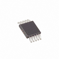
MAX3208EAUB+ Maxim Integrated Products, MAX3208EAUB+ Datasheet - Page 2

MAX3208EAUB+
Manufacturer Part Number
MAX3208EAUB+
Description
IC ESD PROT DIFF 10-UMAX
Manufacturer
Maxim Integrated Products
Type
Diode Arraysr
Series
MAX3208Er
Datasheet
1.MAX3208EAUB.pdf
(9 pages)
Specifications of MAX3208EAUB+
Power (watts)
444mW
Polarization
4 Channel Array - Unidirectional
Mounting Type
Surface Mount
Package / Case
10-MSOP, Micro10™, 10-uMAX, 10-uSOP
Capacitance Value
10(Typ) pF
Maximum Clamping Voltage
105.5 V
Number Of Elements Per Chip
4
Esd Protection Voltage
±15@HBM|±15@Air Gap|±8@Contact Disc KV
Maximum Leakage Current
0.1 uA
Channels
4 Channels
Clamping Voltage
100 V
Operating Voltage
- 0.3 V to + 6.0 V
Termination Style
SMD/SMT
Capacitance
2 pF
Maximum Operating Temperature
+ 125 C
Minimum Operating Temperature
- 40 C
Dimensions
3.05 (Max) mm W x 3.05 (Max) mm L
Diode Type
ESD Protection
Power Dissipation Pd
444mW
Diode Case Style
µMAX
No. Of Pins
10
Termination Type
SMD
Capacitance, Cd
2.6pF
Operating Temperature Range
-40°C To +125°C
Rohs Compliant
Yes
Filter Terminals
SMD
Esd Threat Voltage Max
15kV
Lead Free Status / RoHS Status
Lead free / RoHS Compliant
Voltage - Breakdown
-
Voltage - Reverse Standoff (typ)
-
Lead Free Status / Rohs Status
Lead free / RoHS Compliant
ABSOLUTE MAXIMUM RATINGS
V
I/O_ to GND ................................................-0.3V to (V
Continuous Power Dissipation (T
Dual, Quad, and Hex High-Speed
Differential ESD-Protection ICs
Stresses beyond those listed under “Absolute Maximum Ratings” may cause permanent damage to the device. These are stress ratings only, and functional
operation of the device at these or any other conditions beyond those indicated in the operational sections of the specifications is not implied. Exposure to
absolute maximum rating conditions for extended periods may affect device reliability.
ELECTRICAL CHARACTERISTICS
(V
2
Note 1: Parameters are 100% production tested at +25°C. Limits over temperature are guaranteed by design only.
Note 2: Idealized clamp voltages. See the Applications Information section for more information.
Note 3: Guaranteed by design, not production tested.
Supply Voltage
Supply Current
Diode Forward Voltage
Channel Clamp Voltage
(Note 2)
Channel Leakage Current
Channel I/O Capacitance
Channel I/O to I/O
Variation in Capacitance
TRANSIENT SUPPRESSOR
V
ESD Trigger Voltage
CC
CC
CC
6-Pin SOT23 (derate 8.7mW/°C above +70°C)............696mW
9-Bump WLP (derate 14.1mW/°C above +70°C).............0mW
10-Pin µMAX (derate 5.6mW/°C above +70°C) ...........444mW
16-Pin TQFN (derate 20.8mW/°C above +70°C) .......1667mW
_______________________________________________________________________________________
to GND ...........................................................-0.3V to +6.0V
Capacitance to GND
= +5V, T
PARAMETER
A
= T
MIN
to T
MAX
SYMBOL
, unless otherwise noted. Typical values are at V
V
A
I
V
CC
V
C
CC
= +70°C)
C
F
IN
I
T
Body Model, I
T
Discharge (IEC 61000-4-2),
I
T
Discharge (IEC 61000-4-2),
I
V
V
dV/dt 1V/ns (Note 3)
F
F
F
A
A
A
CC
CC
= 10mA
= 24A
= 45A
= +25°C, ±15kV Human
= +25°C, ±15kV Air-Gap
= +25°C, ±8kV Contact
= +3.3V, bias of V
= +3.3V, bias of V
CC
F
+ 0.3V)
= 10A
CONDITIONS
CC
CC
/ 2
/ 2, C
Operating Temperature Range .........................-40°C to +125°C
Storage Temperature Range .............................-65°C to +150°C
Junction Temperature .....................................................+150°C
Lead Temperature (excluding WLP; soldering, 10s) .......+300°C
Soldering Temperature (reflow) .......................................+260°C
Positive transients
Negative transients
Positive transients
Negative transients
Positive transients
Negative transients
MAX3205EAWL+T
MAX3207EAUT+T
MAX3205EATE+
MAX3208EATE+
MAX3208EAUB+
I/O_
to GND
CC
= +5V and T
0.65
MIN
-0.1
0.9
A
= +25°C.) (Note 1)
±0.05
TYP
2.5
2.7
2.6
10
1
9
V
V
V
CC
CC
CC
MAX
-100
+0.1
0.95
100
5.5
3.2
3.1
-25
-60
+ 100
3
+ 25
+ 60
UNITS
nA
μA
pF
pF
pF
V
V
V
V


