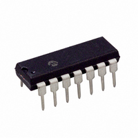
PIC16F616-I/P Microchip Technology, PIC16F616-I/P Datasheet - Page 90

PIC16F616-I/P
Manufacturer Part Number
PIC16F616-I/P
Description
IC PIC MCU FLASH 2KX14 14DIP
Manufacturer
Microchip Technology
Series
PIC® 16Fr
Datasheets
1.PIC12F609T-ISN.pdf
(26 pages)
2.PIC16F616T-ISL.pdf
(4 pages)
3.PIC16F616T-ISL.pdf
(214 pages)
4.PIC16F616T-ISL.pdf
(8 pages)
5.PIC16F616-ESL.pdf
(180 pages)
Specifications of PIC16F616-I/P
Core Size
8-Bit
Program Memory Size
3.5KB (2K x 14)
Peripherals
Brown-out Detect/Reset, POR, PWM, WDT
Core Processor
PIC
Speed
20MHz
Number Of I /o
11
Program Memory Type
FLASH
Ram Size
128 x 8
Voltage - Supply (vcc/vdd)
2 V ~ 5.5 V
Data Converters
A/D 8x10b
Oscillator Type
Internal
Operating Temperature
-40°C ~ 85°C
Package / Case
14-DIP (0.300", 7.62mm)
Controller Family/series
PIC16F
No. Of I/o's
12
Ram Memory Size
128Byte
Cpu Speed
20MHz
No. Of Timers
3
Package
14PDIP
Device Core
PIC
Family Name
PIC16
Maximum Speed
20 MHz
Operating Supply Voltage
2.5|3.3|5 V
Data Bus Width
8 Bit
Number Of Programmable I/os
11
On-chip Adc
8-chx10-bit
Number Of Timers
3
Processor Series
PIC16F
Core
PIC
Data Ram Size
128 B
Maximum Clock Frequency
20 MHz
Maximum Operating Temperature
+ 85 C
Mounting Style
Through Hole
3rd Party Development Tools
52715-96, 52716-328, 52717-734
Development Tools By Supplier
PG164130, DV164035, DV244005, DV164005, PG164120, ICE2000
Minimum Operating Temperature
- 40 C
Lead Free Status / RoHS Status
Lead free / RoHS Compliant
For Use With
MCP1631RD-DCPC1 - REF DES BATT CHARG OR LED DRIVERAC162083 - HEADER MPLAB ICD2 PIC16F616 8/14AC124001 - MODULE SKT PROMATEII 8DIP/SOIC
Eeprom Size
-
Connectivity
-
Lead Free Status / Rohs Status
Details
PIC16F610/616/16HV610/616
10.3
The PWM mode generates a Pulse-Width Modulated
signal on the CCP1 pin. The duty cycle, period and
resolution are determined by the following registers:
• PR2
• T2CON
• CCPR1L
• CCP1CON
In Pulse-Width Modulation (PWM) mode, the CCP
module produces up to a 10-bit resolution PWM output
on the CCP1 pin. Since the CCP1 pin is multiplexed
with the PORT data latch, the TRIS for that pin must be
cleared to make the CCP1 pin an output.
Figure 10-3 shows a simplified block diagram of PWM
operation.
Figure 10-4 shows a typical waveform of the PWM
signal.
For a step-by-step procedure on how to set up the CCP
module for PWM operation, see Section 10.3.7
“Setup for PWM Operation”.
FIGURE 10-3:
DS41288C-page 88
Note 1:
Note:
CCPR1H
Duty Cycle Registers
Comparator
2:
CCPR1L
PWM Mode
PR2
TMR2
Comparator
Clearing the CCP1CON register will
relinquish CCP1 control of the CCP1 pin.
The 8-bit timer TMR2 register is concatenated
with the 2-bit internal system clock (F
2 bits of the prescaler, to create the 10-bit time
base.
In PWM mode, CCPR1H is a read-only register.
(2)
(Slave)
(1)
SIMPLIFIED PWM BLOCK
DIAGRAM
Clear Timer2,
toggle CCP1 pin and
latch duty cycle
CCP1CON<5:4>
S
R
Q
TRIS
OSC
CCP1
), or
Preliminary
The PWM output (Figure 10-4) has a time base
(period) and a time that the output stays high (duty
cycle).
FIGURE 10-4:
Pulse Width
TMR2 = 0
Period
CCP PWM OUTPUT
TMR2 = CCPR1L:CCP1CON<5:4>
© 2007 Microchip Technology Inc.
TMR2 = PR2


