PIC16F677-I/P Microchip Technology, PIC16F677-I/P Datasheet - Page 175
PIC16F677-I/P
Manufacturer Part Number
PIC16F677-I/P
Description
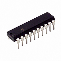
IC PIC MCU FLASH 2KX14 20DIP
Manufacturer
Microchip Technology
Series
PIC® 16Fr
Datasheets
1.PIC16F616T-ISL.pdf
(8 pages)
2.PIC16F690DM-PCTLHS.pdf
(306 pages)
3.PIC16F677-IP.pdf
(2 pages)
4.PIC16F677-IP.pdf
(16 pages)
5.PIC16F677-ISO.pdf
(294 pages)
Specifications of PIC16F677-I/P
Program Memory Type
FLASH
Program Memory Size
3.5KB (2K x 14)
Package / Case
20-DIP (0.300", 7.62mm)
Mfg Application Notes
Intro to Capacitive Sensing Appl Notes Layout and Physical Design Appl Note
Core Processor
PIC
Core Size
8-Bit
Speed
20MHz
Connectivity
I²C, SPI
Peripherals
Brown-out Detect/Reset, POR, WDT
Number Of I /o
18
Eeprom Size
256 x 8
Ram Size
128 x 8
Voltage - Supply (vcc/vdd)
2 V ~ 5.5 V
Data Converters
A/D 12x10b
Oscillator Type
Internal
Operating Temperature
-40°C ~ 85°C
Processor Series
PIC16F
Core
PIC
Data Bus Width
8 bit
Data Ram Size
128 B
Interface Type
SSP
Maximum Clock Frequency
20 MHz
Number Of Programmable I/os
17
Number Of Timers
2
Operating Supply Voltage
2 V to 5.5 V
Maximum Operating Temperature
+ 85 C
Mounting Style
Through Hole
3rd Party Development Tools
52715-96, 52716-328, 52717-734
Development Tools By Supplier
PG164130, DV164035, DV244005, DV164005, PG164120, ICE2000, DM163014, DM164120-4
Minimum Operating Temperature
- 40 C
On-chip Adc
12-ch x 10-bit
Lead Free Status / RoHS Status
Lead free / RoHS Compliant
For Use With
AC162061 - HEADER INTRFC MPLAB ICD2 20PINACICE0203 - MPLABICE 20P 300 MIL ADAPTER
Lead Free Status / Rohs Status
Lead free / RoHS Compliant
Available stocks
Company
Part Number
Manufacturer
Quantity
Price
Company:

Part Number:
PIC16F677-I/P
Manufacturer:
MICROCHIP
Quantity:
2 000


12.4.2
The following bits are used to configure the EUSART
for Synchronous slave operation:
• SYNC = 1
• CSRC = 0
• SREN = 0 (for transmit); SREN = 1 (for receive)
• CREN = 0 (for transmit); CREN = 1 (for receive)
• SPEN = 1
Setting the SYNC bit of the TXSTA register configures the
device for synchronous operation. Clearing the CSRC bit
of the TXSTA register configures the device as a slave.
Clearing the SREN and CREN bits of the RCSTA register
ensures that the device is in the Transmit mode,
otherwise the device will be configured to receive. Setting
the SPEN bit of the RCSTA register enables the
EUSART. If the RX/DT or TX/CK pins are shared with an
analog peripheral the analog I/O functions must be
disabled by clearing the corresponding ANSEL bits.
12.4.2.1
The operation of the Synchronous Master and Slave
modes
“Synchronous Master Transmission”), except in the
case of the Sleep mode.
TABLE 12-9:
© 2006 Microchip Technology Inc.
BAUDCTL ABDOVF
INTCON
PIE1
PIR1
RCREG
RCSTA
SPBRG
SPBRGH
TRISB
TXREG
TXSTA
Legend:
Name
are
x = unknown, – = unimplemented read as ‘0’. Shaded cells are not used for Synchronous Slave Transmission.
SYNCHRONOUS SLAVE MODE
EUSART Receive Data Register
EUSART Transmit Data Register
TRISB7
BRG15
SPEN
BRG7
CSRC
EUSART Synchronous Slave
Transmit
Bit 7
GIE
—
—
identical
REGISTERS ASSOCIATED WITH SYNCHRONOUS SLAVE TRANSMISSION
TRISB6
BRG14
RCIDL
BRG6
ADIE
ADIF
Bit 6
PEIE
RX9
TX9
(see
TRISB5
BRG13
SREN
BRG5
TXEN
RCIE
RCIF
Bit 5
T0IE
—
PIC16F631/677/685/687/689/690
Section 12.4.1.3
TRISB4
BRG12
CREN
SCKP
BRG4
SYNC
Bit 4
INTE
TXIE
TXIF
Preliminary
ADDEN
SENDB
BRG16
BRG11
RABIE
SSPIE
SSPIF
BRG3
Bit 3
CCP1IE
CCP1IF
BRG10
BRGH
FERR
BRG2
If two words are written to the TXREG and then the
SLEEP instruction is executed, the following will occur:
1.
2.
3.
4.
5.
12.4.2.2
1.
2.
3.
4.
5.
6.
7.
Bit 2
T0IF
—
The first character will immediately transfer to
the TSR register and transmit.
The second word will remain in TXREG register.
The TXIF bit will not be set.
After the first character has been shifted out of
TSR, the TXREG register will transfer the second
character to the TSR and the TXIF bit will now be
set.
If the PEIE and TXIE bits are set, the interrupt
will wake the device from Sleep and execute the
next instruction. If the GIE bit is also set, the
program will call the interrupt service routine.
Set the SYNC and SPEN bits and clear the
CSRC bit.
Clear the CREN and SREN bits.
If using interrupts, ensure that the GIE and PEIE
bits of the INTCON register are set and set the
TXIE bit.
If 9-bit transmission is desired, set the TX9 bit.
Enable transmission by setting the TXEN bit.
If 9-bit transmission is selected, insert the Most
Significant bit into the TX9D bit.
Start
Significant 8 bits to the TXREG register.
TMR2IE
TMR2IF
OERR
BRG1
BRG9
TRMT
WUE
Bit 1
INTF
transmission
Synchronous Slave Transmission
Set-up:
TMR1IE
TMR1IF
ABDEN
RABIF
RX9D
BRG0
BRG8
TX9D
Bit 0
by
01-0 0-00
0000 000x
-000 0000
-000 0000
0000 0000
0000 000x
0000 0000
0000 0000
1111 ----
0000 0000
0000 0010
POR, BOR
Value on
writing
DS41262C-page 173
the
01-0 0-00
0000 000x
-000 0000
-000 0000
0000 0000
0000 000x
0000 0000
0000 0000
1111 ----
0000 0000
0000 0010
Value on
all other
Resets
Least
Related parts for PIC16F677-I/P
Image
Part Number
Description
Manufacturer
Datasheet
Request
R

Part Number:
Description:
3.5KB Flash, 128B RAM, 18 I/O, CLC, CWG, DDS, 10-bit ADC 20 QFN 4x4mm TUBE
Manufacturer:
Microchip Technology
Datasheet:

Part Number:
Description:
3.5KB Flash, 128B RAM, 18 I/O, CLC, CWG, DDS, 10-bit ADC 20 PDIP .300in TUBE
Manufacturer:
Microchip Technology
Datasheet:

Part Number:
Description:
3.5KB Flash, 128B RAM, 18 I/O, CLC, CWG, DDS, 10-bit ADC 20 SOIC .300in TUBE
Manufacturer:
Microchip Technology
Datasheet:

Part Number:
Description:
3.5KB Flash, 128B RAM, 18 I/O, CLC, CWG, DDS, 10-bit ADC 20 SSOP .209in TUBE
Manufacturer:
Microchip Technology
Datasheet:
Part Number:
Description:
3.5KB Flash, 128B RAM, 18 I/O, CLC, CWG, DDS, 10-bit ADC 20 QFN 4x4mm TUBE
Manufacturer:
Microchip Technology
Datasheet:
Part Number:
Description:
3.5KB Flash, 128B RAM, 18 I/O, CLC, CWG, DDS, 10-bit ADC 20 PDIP .300in TUBE
Manufacturer:
Microchip Technology
Datasheet:
Part Number:
Description:
3.5KB Flash, 128B RAM, 18 I/O, CLC, CWG, DDS, 10-bit ADC 20 SOIC .300in TUBE
Manufacturer:
Microchip Technology
Datasheet:
Part Number:
Description:
3.5KB Flash, 128B RAM, 18 I/O, CLC, CWG, DDS, 10-bit ADC 20 SSOP .209in TUBE
Manufacturer:
Microchip Technology
Datasheet:
Part Number:
Description:
3.5KB Flash, 128B RAM, 18 I/O, CLC, CWG, DDS, 10-bit ADC 20 QFN 4x4mm T/R
Manufacturer:
Microchip Technology
Datasheet:
Part Number:
Description:
3.5KB Flash, 128B RAM, 18 I/O, CLC, CWG, DDS, 10-bit ADC 20 SOIC .300in T/R
Manufacturer:
Microchip Technology
Datasheet:
Part Number:
Description:
3.5KB Flash, 128B RAM, 18 I/O, CLC, CWG, DDS, 10-bit ADC 20 SSOP .209in T/R
Manufacturer:
Microchip Technology
Datasheet:
Part Number:
Description:
3.5KB Flash, 128B RAM, 18 I/O, CLC, CWG, DDS, 10-bit ADC 20 QFN 4x4mm TUBE
Manufacturer:
Microchip Technology
Datasheet:
Part Number:
Description:
3.5KB Flash, 128B RAM, 18 I/O, CLC, CWG, DDS, 10-bit ADC 20 PDIP .300in TUBE
Manufacturer:
Microchip Technology
Datasheet:
Part Number:
Description:
3.5KB Flash, 128B RAM, 18 I/O, CLC, CWG, DDS, 10-bit ADC 20 SOIC .300in TUBE
Manufacturer:
Microchip Technology
Datasheet:
Part Number:
Description:
3.5KB Flash, 128B RAM, 18 I/O, CLC, CWG, DDS, 10-bit ADC 20 SSOP .209in TUBE
Manufacturer:
Microchip Technology
Datasheet: