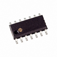
PIC16F630-I/SL Microchip Technology, PIC16F630-I/SL Datasheet - Page 25

PIC16F630-I/SL
Manufacturer Part Number
PIC16F630-I/SL
Description
IC MCU FLASH 1KX14 EEPROM 14SOIC
Manufacturer
Microchip Technology
Series
PIC® 16Fr
Datasheets
1.PIC16F616T-ISL.pdf
(8 pages)
2.PIC12F629T-ISN.pdf
(24 pages)
3.PIC16F630-ISL.pdf
(132 pages)
4.PIC16F630-ISL.pdf
(2 pages)
5.PIC16F630-ISL.pdf
(10 pages)
6.PIC16F676-EP.pdf
(132 pages)
7.PIC16F676-ISL.pdf
(130 pages)
Specifications of PIC16F630-I/SL
Program Memory Type
FLASH
Program Memory Size
1.75KB (1K x 14)
Package / Case
14-SOIC (3.9mm Width), 14-SOL
Core Processor
PIC
Core Size
8-Bit
Speed
20MHz
Peripherals
Brown-out Detect/Reset, POR, WDT
Number Of I /o
12
Eeprom Size
128 x 8
Ram Size
64 x 8
Voltage - Supply (vcc/vdd)
2 V ~ 5.5 V
Oscillator Type
Internal
Operating Temperature
-40°C ~ 85°C
Processor Series
PIC16F
Core
PIC
Data Bus Width
8 bit
Data Ram Size
64 B
Interface Type
RS- 232/USB
Maximum Clock Frequency
20 MHz
Number Of Programmable I/os
12
Number Of Timers
2
Operating Supply Voltage
2 V to 5.5 V
Maximum Operating Temperature
+ 85 C
Mounting Style
SMD/SMT
3rd Party Development Tools
52715-96, 52716-328, 52717-734
Development Tools By Supplier
PG164130, DV164035, DV244005, DV164005, PG164120, ICE2000, DM163014, DM164120-4
Minimum Operating Temperature
- 40 C
Package
14SOIC N
Device Core
PIC
Family Name
PIC16
Maximum Speed
20 MHz
Lead Free Status / RoHS Status
Lead free / RoHS Compliant
Data Converters
-
Connectivity
-
Lead Free Status / Rohs Status
Lead free / RoHS Compliant
Available stocks
Company
Part Number
Manufacturer
Quantity
Price
Company:
Part Number:
PIC16F630-I/SL
Manufacturer:
TriQuint
Quantity:
1 200
Company:
Part Number:
PIC16F630-I/SL
Manufacturer:
MICROCHI
Quantity:
1 743
Part Number:
PIC16F630-I/SL
Manufacturer:
MICROCHIP/微芯
Quantity:
20 000
3.2.3.3
Figure 3-2 shows the diagram for this pin. The RA2 pin
is configurable to function as one of the following:
• a general purpose I/O
• an analog input for the A/D (PIC16F676 only)
• a digital output from the comparator
• the clock input for TMR0
• an external edge triggered interrupt
FIGURE 3-2:
© 2007 Microchip Technology Inc.
PORTA
PORTA
Data Bus
WPUA
WPUA
TRISA
TRISA
Interrupt-on-Change
IOCA
IOCA
WR
WR
WR
WR
RD
RD
RD
RD
D
D
D
D
To TMR0
To INT
To A/D Converter
CK
CK
CK
CK
RA2/AN2/T0CKI/INT/COUT
Q
Q
Q
Q
Q
Q
Q
Q
Input Mode
BLOCK DIAGRAM OF RA2
Analog
Enable
COUT
COUT
RAPU
Input Mode
RD PORTA
Analog
1
0
Q
Q
Analog
Mode
Input
EN
EN
D
D
V
DD
Weak
V
V
DD
SS
I/O pin
3.2.3.4
Figure 3-3 shows the diagram for this pin. The RA3 pin
is configurable to function as one of the following:
• a general purpose input
• as Master Clear Reset
FIGURE 3-3:
Data Bus
PORTA
Interrupt-on-Change
IOCA
IOCA
TRISA
WR
RD
RD
RD
D
CK
RA3/MCLR/V
PIC16F630/676
Q
Q
RESET
BLOCK DIAGRAM OF RA3
V
SS
PP
RD PORTA
MCLRE
Q
Q
MCLRE
EN
EN
DS40039E-page 23
D
D
V
SS
I/O pin


